


AFM Pioneers Honored with Kavli Prize in Nanoscience
After 30 years and more than 9,000 citations, the inventors of the Atomic Force Microscope (AFM) have been awarded the Kavli Prize in Nanoscience.
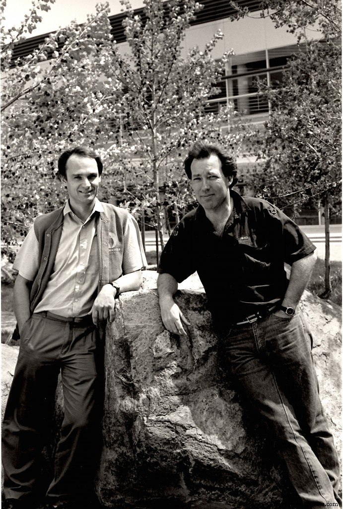
Gerd Binnig and Christoph Gerber in the 1990s.
The Kavli Prize is shared between Gerd Binnig, Christoph Gerber and Calvin Quate. Binnig and Gerber were previously based at IBM Research – Zurich, while Quate was at Stanford University. During a sabbatical, Binnig was at Stanford and Gerber at IBM Research in San Jose (now Almaden), fostering close collaboration.
The three scientists were honored “for the invention and realization of atomic force microscopy, a breakthrough in measurement technology and nanosculpting that continues to have a transformative impact on nanoscience and technology.”
The AFM was first described in a 3 March 1986 issue of Physical Review Letters under the concise title “Atomic Force Microscope.” The device combined the principles of scanning tunnelling microscopy (STM) with a stylus profilometer, enabling atomic‑resolution imaging.
Binnig, who also co‑invented the STM with the late Heinrich Rohrer, received the Nobel Prize in Physics in 1986 for that work. He later credited the AFM idea to a subconscious insight he had while lying on a couch, as noted in a 2004 interview in IEEE Spectrum Magazine.
During his time at Stanford, Binnig enlisted the expertise of Calvin Quate and his IBM colleague Christoph Gerber—who had previously collaborated on the STM—to bring the AFM from concept to reality.
In a recent interview with Physics World marking the 30th anniversary, Gerber reflected on the invention’s evolution:
“Gerd suggested that we might measure the interactive forces between tip and sample, rather than the tunnelling current, and that a cantilever could do this. We did a rough calculation and realized that achieving atomic resolution required detecting forces at the level of 10–10 N or even 10–11 N!”
The ability to sense such minuscule forces hinged on two key materials: gold and diamond. Gerber explained:
“The heart of the device was a very thin gold foil, only a few microns thick, used as a cantilever. We attached a fragment from a crushed diamond—originally from a record‑player stylus—to the cantilever to serve as the tip.”
While atomic resolution was not achieved immediately, the team was close enough to submit a paper. Within a year they developed a batch‑fabricated silicon cantilever that produced the first atomic‑resolution images on a graphite surface.
After this milestone, the trio pushed AFM technology in new directions, especially in cantilever design and application.
Binnig pioneered a massively parallel probe for nanostructuring, aimed at developing non‑volatile memory. His work spurred a wave of innovations in nanopatterning techniques.
Gerber advanced an “artificial nose” using a cantilever array, achieving breakthroughs in chemical, biochemical, and medical diagnostics. He continues this research with his group at the University of Basel, Switzerland.
Quate focused on micromechanical cantilevers for sensing applications in drug discovery, food diagnostics, material characterization, and explosives detection.
Over the past three decades, AFM instruments have evolved dramatically, improving sensitivity and resolution while expanding into diverse fields.
In 2008, Markus Ternes and colleagues at IBM Research – Almaden used the AFM to slide single atoms across a surface and directly measure the forces involved.
The following year, a team from IBM Research – Zurich, led by Gerhard Meyer and Leo Gross, modified the AFM tip with a single carbon monoxide molecule. This diatomic tip, less than one nanometer long, yielded images that resolved the internal chemical structure of individual molecules—chemical bonds in real time.
Gross noted, “One main differentiator of our technique is that we measure single molecules. Another advantage is that we can use the tip to initiate chemical reactions of individual molecules and track the products at the atomic scale.”
Meyer, Gross, and Bruno Schuler recently published an article on the AFM’s 30th anniversary in Physics World, stating:
“High‑resolution AFM offers opportunities to understand and control physical, chemical, and biological processes at the level of individual molecules. Ongoing improvements in force sensitivity, temporal, and spatial resolution will push the frontiers of nanoscience even further. Perhaps in another 30 years the AFM might evolve toward an atomic assembler, as Richard Feynman envisioned in his 1959 talk “There’s Plenty of Room at the Bottom”—a tool that could build arbitrary, 3D atomically precise devices, metamaterials, and molecules.”
“Regardless, there is no doubt that the AFM will continue to drive discoveries from fundamental physics to chemistry and life sciences, unraveling nature’s most enigmatic mechanisms at the nanometre scale and beyond.”
This is the second Kavli Prize awarded to an IBM scientist. Don Eigler received the 2010 Kavli Prize in Nanoscience for developing atom manipulation and elucidating quantum phenomena with precisely controlled atomic and molecular arrangements on surfaces.
The Kavli Prizes honour scientists who pioneer advances in our understanding of existence at its largest, smallest, and most complex scales. Awarded biennially in astrophysics, nanoscience, and neuroscience, each prize carries a $1 million award (U.S.). Laureates are selected by committees whose members are recommended by six of the world’s most renowned science societies and academies.
Nanomaterials
- Circuit With a Switch: A Practical Guide to Basic Electrical Circuits
- Mastering Multiplication and Division with Scientific Notation
- IBM’s Phase‑Change Artificial Neurons Mimic Brain Spikes for Ultra‑Dense, Low‑Power Computing
- IBM Breakthrough: Controlling a Single Copper Atom’s Magnetism via NMR
- Exfoliation of Trigonal Tellurium: Toward Ultra‑Thin Single‑Atom Chains
- High‑Throughput Nanopit Fabrication on Polymer Thin Films via AFM Dynamic Plowing Lithography
- Hybrid GaAs/AlGaAs Nanowire Laser in Silver V‑Groove Cavities for Advanced Plasmonic Waveguides
- High‑Performance All‑Perovskite Photodetector Delivering Ultrafast Response
- Controlled Low‑Temperature Growth of WSe₂ on Graphene for Efficient p‑Type Transistors
- Build an IR Sensor Project with Arduino UNO – Simple Guide