


Serial‑In, Serial‑Out Shift Registers: Fundamentals and Practical Applications
Shift registers that receive data serially and output it serially are a cornerstone of digital logic design. They delay each bit by one clock period per stage, enabling precise data buffering, serial communication, and clock‑domain crossing.
Each stage stores a single bit, so a single‑stage register holds one bit. When multiple stages are cascaded, the register length grows—up to 64 bits in standard parts, or longer when multiple devices are connected in series.
Below is a single‑stage shift register driven by data that is not yet synchronized to the system clock. The data line (pin D) on a D‑flip‑flop (D‑FF) holds its value until the clock edge, after which the value appears on the output pin Q.
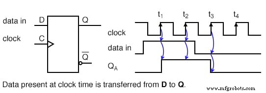
The key point—unlike the next figure—is that the data present at the D pin is transferred to Q precisely at the rising edge of the clock. Because the input is stable well before and after the edge, the flip‑flop captures the correct value.
For positive‑edge‑triggered flip‑flops, the output follows the input immediately after the clock transition, as shown by the upward arrows.
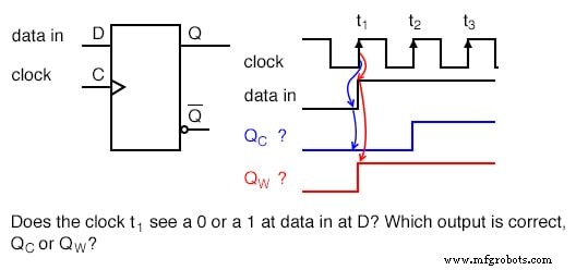
In multi‑stage shift registers, the data at the input may change near the clock edge. In such cases, the flip‑flop still samples the value present just before the edge; any change that occurs at the edge is ignored until the next clock pulse.
Consequently, a D‑FF acts as a one‑clock‑period delay element, provided the data is properly synchronized to the clock. The output waveform is a delayed copy of the input, shifted by one clock cycle.
To illustrate the timing, consider the CD4006B 18‑bit serial‑in, serial‑out shift register from Texas Instruments. Its datasheet specifies operation at 5 V DC with the following key parameters:
- Setup time (tS) = 100 ns
- Hold time (tH) = 60 ns
- Propagation delay (tP) = 200–400 ns (typical/maximum)
These values ensure that data presented on the D pin is stable at least 100 ns before the clock edge and remains unchanged for 60 ns afterward. With a 1 MHz clock (1 µs period), the setup and hold margins are comfortably satisfied.
When cascaded, each stage’s output (Q) feeds the next stage’s input (D). Because the propagation delay (200 ns) exceeds the hold time, the data remains valid throughout the transition, guaranteeing reliable operation.
The same concept applies to JK‑flip‑flops, where Q feeds J and Q’ feeds K to form an equivalent shift register.
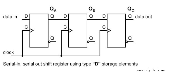
A serial‑in, serial‑out (SISO) shift register has a single data input, a clock input, and a single output that appears on the last stage. The intermediate outputs are typically not exposed, distinguishing it from a serial‑in, parallel‑out (SIPO) register.
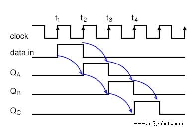
For a three‑stage SISO register, the following waveforms demonstrate how three bits propagate through the stages, each delayed by one clock cycle.
Serial‑In, Serial‑Out Devices from Texas Instruments
The following Texas Instruments parts illustrate the concepts discussed above:
- CD4006B – 18‑bit SISO shift register
- CD4031B – 64‑bit SISO shift register
- CD4517B – Dual 64‑bit SISO shift register with internal taps
These are 4000‑series CMOS devices, operating from 3 V to 15 V on the positive supply (VDD), with VSS grounded. Typical maximum clock frequencies are a few megahertz, depending on supply voltage.
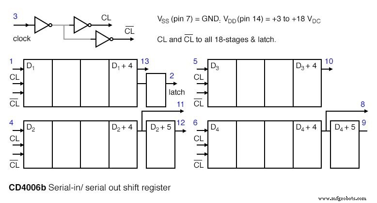
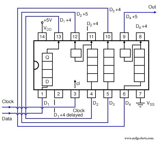
The CD4006B can be configured as an 18‑bit register by cascading its internal 4‑bit and 5‑bit stages. Its internal tap allows a 4‑bit output for applications that require a shorter shift register.
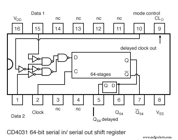
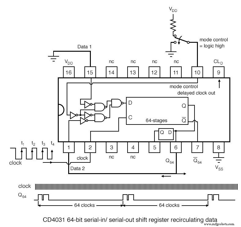
The CD4031B offers a full 64‑bit SISO shift register. It includes two additional outputs—Q64 and Q64’—and a half‑stage delayed output that lags by half a clock cycle. A mode‑control input selects between two data sources (data 1 or data 2), enabling data recirculation when desired.
When mode‑control is high, the output Q64 is routed back into the data input, creating a 64‑cycle feedback loop. This can be useful for implementing repeating patterns or circular buffers.
The CD4517B provides two independent 64‑bit shift registers (sections A and B). Each section has its own clock, data input, and write enable (WE). Internal taps at 16, 32, and 48 stages allow flexible reconfiguration for 16‑bit, 32‑bit, or 48‑bit registers.
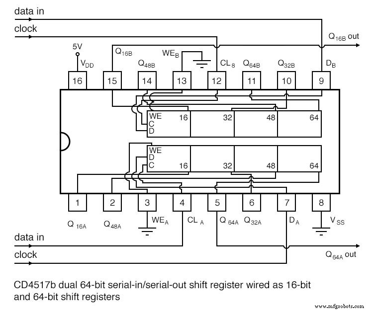
For example, configuring section B as a 16‑bit register involves tying WEB to ground, supplying clock on CLB, and reading the delayed output from Q16B. Section A can be used simultaneously as a full 64‑bit register by following the same principle.
RELATED WORKSHEETS
Industrial Technology
- Low‑Voltage AC Power Supply: Phase‑Shift Circuit Components & Best Practices
- Shift Registers: Fundamentals, Applications, and Design Variants
- Parallel‑to‑Serial Shift Registers (PISO): Design, Operation, and Applications
- Serial‑In, Parallel‑Out Shift Registers: Converting Serial Data to Parallel for Efficient I/O Expansion
- Universal Shift Registers: Parallel‑In/Parallel‑Out with Bidirectional Shift Control
- Understanding Network Protocols: From Physical Layer to Advanced Arbitration
- Microprocessors: The Evolution of Stored‑Program Computing
- Comprehensive Op-Amp Data: National Semiconductor & CA3130 Datasheets
- Understanding AC Phase Shift: How Waveforms Lead and Lag
- Controlling 32 LEDs with Arduino Nano and 4x 74HC595 Shift Registers – A Beginner’s Guide