


Universal Shift Registers: Parallel‑In/Parallel‑Out with Bidirectional Shift Control
A parallel‑in/parallel‑out shift register accepts data in parallel, shifts it, and presents the shifted result, as illustrated below.
A universal shift register expands this capability by supporting parallel loading, serial shifting, and additional control options such as direction and hold modes.
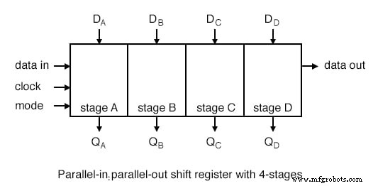
In the figure above, four bits of data are applied to the parallel inputs DA DB DC DD. The mode control signals determine whether the data is loaded in parallel or shifted one position per clock pulse.
Many devices allow the same control line to select the shift direction. Each clock transition moves the data one bit; the shifted output is available on QA QB QC QD. The “data‑in” and “data‑out” pins facilitate cascading multiple registers.
While the diagram shows only right‑shift cascading, left‑shift cascades can be accommodated by adding a second pair of “data‑in” and “data‑out” pins oriented to the left.
The internal structure of a right‑shifting parallel‑in/parallel‑out shift register is shown below. Tri‑state buffers are optional but common in commercial parts.
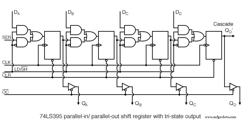
The 74LS395 is a prime example that closely matches the conceptual diagram above. An abbreviated datasheet summary follows; the full datasheet is linked later in this chapter.
LD/SH’ controls the multiplexer that selects between parallel loading and serial shifting. When LD/SH’ = 1, the upper four AND gates enable the parallel inputs DA DB DC DD to enter the four flip‑flops. The clock input is inverted, so data is latched on the negative edge.
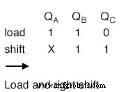
With the register loaded, setting LD/SH’ = 0 activates the shift path, moving the contents one bit to the right on each negative‑edge clock. After four clocks the data will have exited the register unless it is cascaded via QD’ to the serial input of another device.
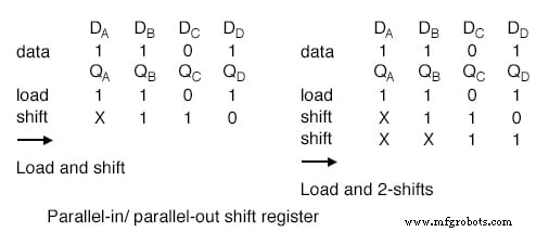
The diagram shows a data pattern loaded into QA QB QC QD and then shifted one position to the right. The incoming bit is unknown (marked X); grounding the SER pin would make the input logic level clear.
Two‑clock shifting (two‑bit shift) is illustrated in the following figure.
These schematic references are kept concise because the essential functionality is already covered in the subsequent, more detailed figures.
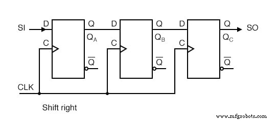
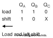
For a left‑shift configuration, the flip‑flops must be rewired, swapping the serial input (SI) and serial output (SO) pins. The data path becomes: SI → QC → QB → QA → SO, which is the reverse of the right‑shift sequence.
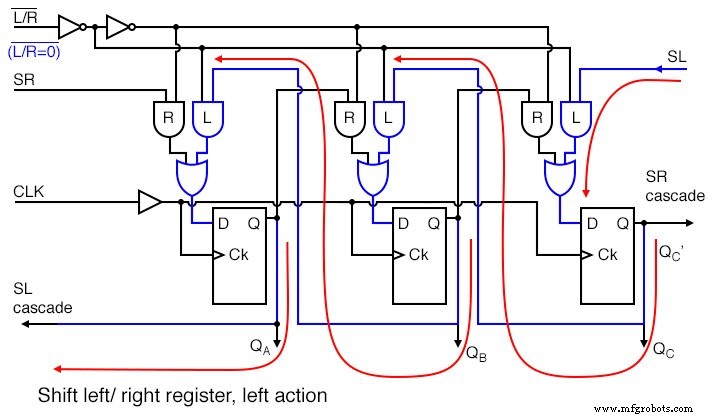
Commercial devices typically implement bidirectional shifting by adding a control line (L/R). The following schematic demonstrates a hypothetical register that can shift left or right depending on the L/R signal.
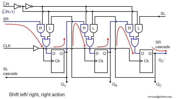
With L/R = 1, the multiplexer enables the right‑shift path; L/R = 0 selects the left‑shift path. The serial data input (SR for right, SL for left) feeds into the first flip‑flop, and the serial output (SR cascade or SL cascade) provides the data leaving the register.
To combine parallel loading with bidirectional shifting, a third control line (SH/LD’) is introduced. When SH/LD’ = 0, the load multiplexer passes the parallel inputs DA DB DC to the flip‑flops on the next clock. Setting SH/LD’ = 1 disables the load path and re‑enables the shift control determined by L/R.
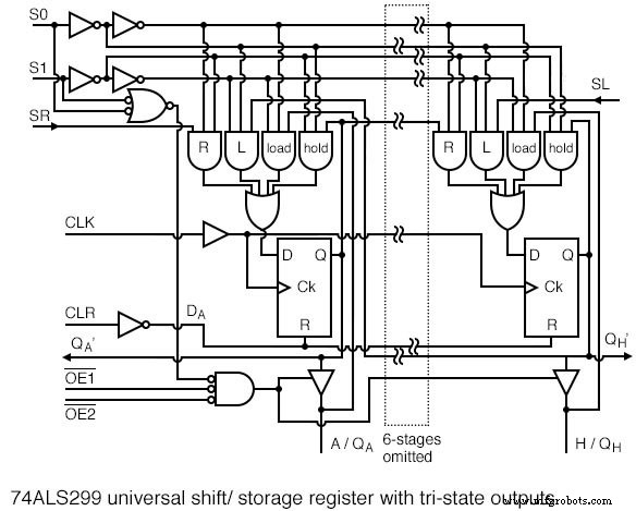
Commercial implementations, such as the 74ALS299, add an additional AND gate to support a hold mode (S1 S0 = 00), which continuously reloads the output on each clock, preserving the stored data.
See the next section for the 74ALS299 schematic.
Parallel‑In / Parallel‑Out and Universal Devices
Texas Instruments offers a range of serial‑in/parallel‑out shift registers. Refer to the links below for complete datasheets.
- SN74LS395A – 4‑bit parallel‑in/parallel‑out shift register
- SN74ALS299 – 8‑bit parallel‑in/parallel‑out universal shift register
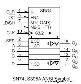
The internal schematic of the SN74LS395A is shown above. The ANSI symbol is presented in the next figure.
The 4‑bit device is limited by the 16‑pin DIP package, which must accommodate the four data pins, control pins, and power pins.
Key control signals include:
- CLR’ – active‑low reset for all stages.
- OC’ – active‑low enable for the four tristate output buffers.
- LD/SH’ – multiplexes between parallel load (M1) and serial shift (M2).
- C3/2 – a negative‑edge clock that clocks both the parallel data (via 3 prefixed signals) and the serial data (via 2 prefixed signals).
Tri‑state buffers are controlled by the EN4 signal (low enables all four buffers). When QD’ is cascaded to another device’s SER pin, data can be shifted through multiple registers.
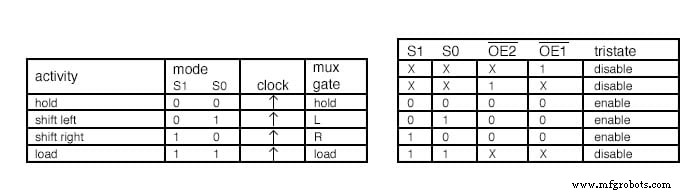
The table above, derived from the 74ALS299 datasheet, summarizes the operation of the 8‑bit universal shift register. The mode inputs S1 and S0 select one of four functions:
- 01 – shift left
- 10 – shift right
- 11 – parallel load
- 00 – hold (continuous re‑load of the output on each clock)
In hold mode, the data bus is tri‑stated to allow external devices to drive the bus while the register preserves its contents.
When S1 S0 = 00, 01, or 10 and the output enable signals OE2’, OE1’ are low, the shift register’s outputs are driven onto the bus.
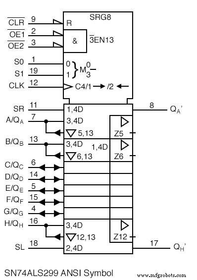
The right‑shift sequence (S1 S0 = 10) is: SR → QA → QB → QC → QD → QE → QF → QG → QH (QH’).
The left‑shift sequence (S1 S0 = 01) is: (QA’) → QA ← QB ← QC ← QD ← QE ← QF ← QG ← QH (QSL’).
Tri‑state buffers can be disabled by asserting either OE2’ or OE1’; the internal register contents remain unchanged but are not visible on the output pins.
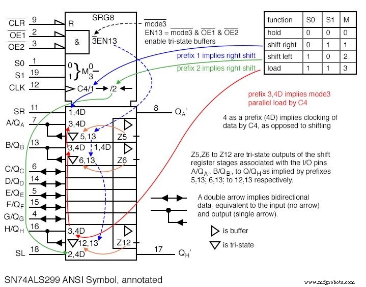
The annotated ANSI symbol clarifies the naming conventions used in the datasheet. Note that the mode bits S0 S1 are listed in reverse order relative to the table above, a quirk of the official documentation.
Practical Applications
The following example demonstrates how a universal shift register can consolidate a remote keypad and LED display into a single device for an alarm system.
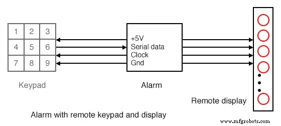
In the diagram, the keypad and display are housed within the same enclosure. Keyboard data is parallel‑loaded into the shift register on a single clock pulse, then serially shifted to the main alarm box. Simultaneously, LED data from the main box is serially loaded into the register to drive the LEDs.
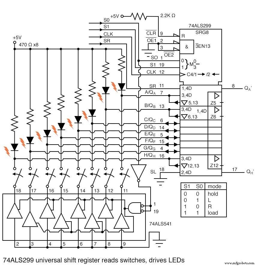
Eight LEDs and current‑limiting resistors are connected to the eight I/O pins of the SN74ALS299. LEDs can only be driven in Mode 3 (S1 = 0, S0 = 0) when the tristate enables OE1’ and OE2’ are grounded, permanently enabling the outputs during Modes 0, 1, and 2. If flicker during shifting is undesirable, the enables can be tied to the mode bits so that the LEDs light only in hold mode.
During parallel loading, setting S0 = 1 (logic 0 after inversion) activates the tristate buffers to pull the switch contacts to ground. The open contacts are pulled high by the resistor‑LED network, creating a clear logic high when no key is pressed.
At time t0, when both S0 and S1 are high, the switch data is loaded into the register. Afterward, eight clock pulses (t0 to t8) shift the switch closure data out via QH’, while new LED data is shifted in at SR of the register.
After the eighth shift (t8), S1 goes low, placing the register in hold mode (S1 S0 = 00). The stored data remains stable even if additional clocks are applied.
Clock generation can be handled by a microcontroller if the rate is below 100 kHz; for higher frequencies, dedicated logic can produce the necessary clocks and mode signals.
Related Worksheets:
- Shift Registers Worksheet
Industrial Technology
- Low‑Voltage AC Power Supply: Phase‑Shift Circuit Components & Best Practices
- Shift Registers: Fundamentals, Applications, and Design Variants
- Serial‑In, Serial‑Out Shift Registers: Fundamentals and Practical Applications
- Parallel‑to‑Serial Shift Registers (PISO): Design, Operation, and Applications
- Serial‑In, Parallel‑Out Shift Registers: Converting Serial Data to Parallel for Efficient I/O Expansion
- Understanding Network Protocols: From Physical Layer to Advanced Arbitration
- Microprocessors: The Evolution of Stored‑Program Computing
- Comprehensive Op-Amp Data: National Semiconductor & CA3130 Datasheets
- Understanding AC Phase Shift: How Waveforms Lead and Lag
- Controlling 32 LEDs with Arduino Nano and 4x 74HC595 Shift Registers – A Beginner’s Guide