


Parallel‑to‑Serial Shift Registers (PISO): Design, Operation, and Applications
Parallel‑to‑Serial (PISO) shift registers expand the functionality of serial‑in/serial‑out (SISO) devices by allowing all stages to load data simultaneously. This capability is essential for converting parallel data—each bit on its own wire—into a serial stream for efficient communication.
A PISO register stores a word of data, then shifts it out one bit per clock cycle, with the total delay equal to the number of stages multiplied by the clock period. Because the data can be loaded in parallel before shifting begins, the register is ideal for high‑speed data acquisition and communication interfaces.
Below is a detailed look at a three‑stage PISO shift register, the core components of which are:
- Type‑D flip‑flops for data storage.
- AND‑OR selectors that choose between parallel loading and serial shifting.
Real‑world devices typically feature 4, 8, or 16 stages. The diagram below illustrates a three‑stage example.
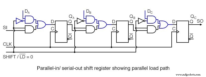
When the SHIFT/LD’ signal is low, the NAND gates on the top enable the parallel load path. Data on inputs D_A, D_B, and D_C is passed to the corresponding D‑flip‑flop inputs. On the next rising clock edge, all three bits are captured simultaneously—a process known as synchronous loading.
Conversely, when SHIFT/LD’ is high, the lower NAND gates activate the shift path: the serial input SI feeds the first stage, each flip‑flop’s output feeds the next stage’s input, and the final output appears on SO. Successive clock edges shift the word right, emitting one bit per cycle.
Waveforms illustrate the transition from parallel loading to serial shifting:
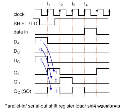
In practice, the SHIFT/LD’ signal must remain low for a brief window around the clock edge to satisfy setup and hold times. A slightly wider pulse is often used for simplicity.
Why include both SI and SO pins? They enable cascading multiple shift registers to create wide shifters or to interface with serial peripherals such as microprocessors and sensors.
Common PISO Devices from Texas Instruments
- SN74ALS166 – 8‑bit, synchronous load
- SN74ALS165 – 8‑bit, asynchronous load
- CD4014B – 8‑bit, synchronous load
- SN74LS647 – 16‑bit, synchronous load
For full device specifications, consult the linked datasheets.
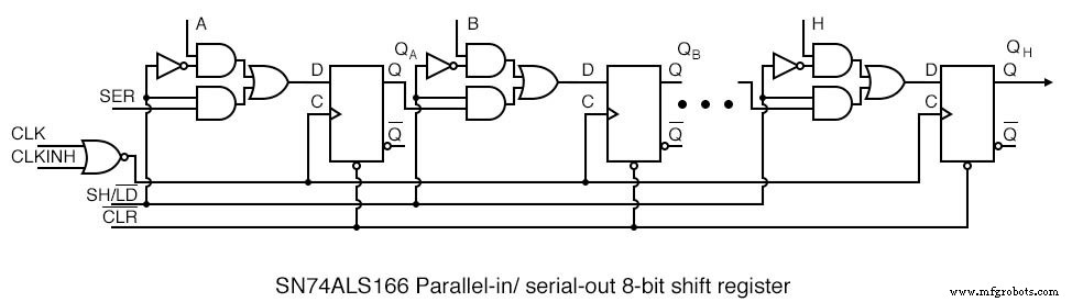
The SN74ALS166, for example, implements an 8‑stage synchronous PISO. Its pins are labeled A–H for data inputs, SER for serial input, SO for serial output, and SH/LD’ for mode control. The CLKINH pin allows the clock to be inhibited when high.
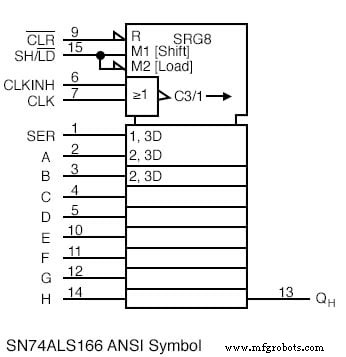
Understanding the ANSI symbol is valuable: the top block houses the mode controls (M1 for shift, M2 for load, C3/1 for clock). The 8‑stage shifter is labeled SRG8, and the serial input SER is governed by the load signal and the clock.
Asynchronous vs. Synchronous Loading
Asynchronous load registers, such as the SN74ALS165, use the flip‑flop’s preset (Set) and clear (Reset) pins to load data independently of the clock. When SH/LD’ is low, the Set pin is driven by the data input while the Reset pin is held high. The data appears immediately in the register, making asynchronous loading useful when a clock pulse is unavailable or unnecessary.
In synchronous devices, the SHIFT/LD’ line controls whether data is loaded or shifted, and the clock synchronizes the action. This mode is preferred in modern designs for its timing predictability.
Practical Applications
One common use of a PISO register is to read a bank of switches or keypads with a microprocessor that has limited I/O pins. For example, a nine‑key keypad can be scanned by a PISO register, reducing the required wires from nine to three.
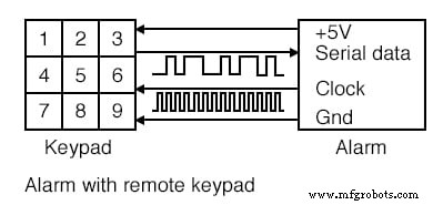
In automotive and industrial settings, this wire‑count reduction improves reliability by minimizing potential points of failure. The shift register’s serial interface also enables communication with other serial devices such as ADCs, sensors, or memory modules.
To implement this, connect the shift register’s parallel inputs to the switch contacts, pull them up to +5V with resistors, and control LD/SH’ from the microprocessor. After loading, generate shift pulses to read each bit from the SO line.
For more complex data streams, cascade additional shift registers or interface with dedicated serial peripherals.
See also: Shift Registers Worksheet
Industrial Technology
- Low‑Voltage AC Power Supply: Phase‑Shift Circuit Components & Best Practices
- Shift Registers: Fundamentals, Applications, and Design Variants
- Serial‑In, Serial‑Out Shift Registers: Fundamentals and Practical Applications
- Serial‑In, Parallel‑Out Shift Registers: Converting Serial Data to Parallel for Efficient I/O Expansion
- Universal Shift Registers: Parallel‑In/Parallel‑Out with Bidirectional Shift Control
- Understanding Network Protocols: From Physical Layer to Advanced Arbitration
- Understanding AC Phase Shift: How Waveforms Lead and Lag
- Mastering Python Type Conversion & Casting: A Comprehensive Guide
- C Typecasting: Mastering Implicit and Explicit Conversions with Code Examples
- Controlling 32 LEDs with Arduino Nano and 4x 74HC595 Shift Registers – A Beginner’s Guide