


Mastering 5‑ and 6‑Variable Karnaugh Maps for Efficient Logic Design
As combinational logic grows, the size of the Karnaugh map expands. Knowing when a 5‑ or 6‑variable map is appropriate—and how to interpret and group its cells—can cut logic usage dramatically in FPGA and ASIC designs.
Altera (now part of Intel) examined thousands of customer designs to understand typical fan‑in sizes. The resulting distribution was almost flat from two to six inputs, with a clear peak at five. In practice, most circuits use no more than six inputs, and the average design comfortably fits within five.
Altera’s own data, extracted from its library of customer designs, supports the value of heterogeneity. By examining logic cones, mapping them onto LUT‑based nodes and sorting them by the number of inputs that would be best at each node, Altera found that the distribution of fan‑ins was nearly flat between two and six inputs, with a nice peak at five.
Below is a classic five‑variable Karnaugh map.
Five Variable K‑map (Reflection Map)
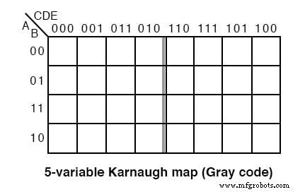
The older reflection style labels the top (and, for a 6‑variable map, the side) of the map with full Gray code. The Gray code is mirrored around the center of the map—a convention found in many classic texts. A newer, preferred layout is shown next.
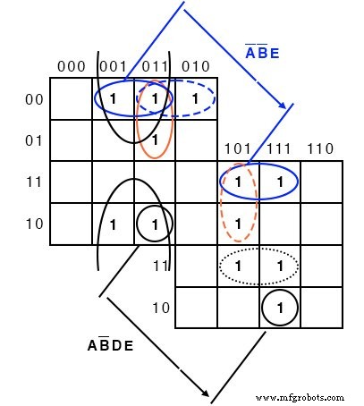
Overlay Version of the K‑map
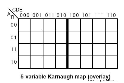
The overlay map consists of two identical 4‑cell sub‑maps, distinguished only by the most‑significant bit of the 3‑bit address across the top. The numbering differs from the reflection map: if the most‑significant digit is ignored, the sequence 00, 01, 11, 10 appears in both sub‑maps. The eight‑bit sequence is not Gray code, but the two‑bit suffix 01, 10 is.
Let’s apply the five‑variable map to a real problem: design a circuit that accepts a 5‑bit binary input (A = MSB, B, C, D, E) and outputs a logic HIGH whenever the binary number is prime.
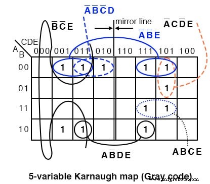
The prime numbers within the 5‑bit range are (1, 2, 3, 5, 7, 11, 13, 17, 19, 23, 29, 31). Mark a 1 in each corresponding cell, then group the ones. Finish by writing the simplified expression.
In the reflection map, the 4‑cell group A’B’E spans two mirror pairs, while the 2‑cell group AB’DE appears as a reflected pair. When using the overlay map, look for mirror images across the two halves.
Out = A’B’E + B’C’E + A’C DE + A’C D’E + ABCE + AB’DE + A’B’C’D
Below is the overlay version of the same expression.
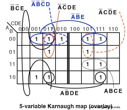
Comparing the two maps, some cells shift because the addressing scheme differs. Overlaying one half atop the other reveals overlapping groups that guide simplification. For example, the 4‑cell group A’B’E covers the pattern ABCDE = 00xx1, meaning A, B, and E are fixed at 0,0,1 respectively while C and D vary.
An example of a six‑variable Karnaugh map follows. By mentally stacking the four sub‑maps, we can identify a 4‑cell group that implements Out = C’F’.
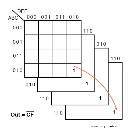
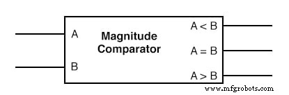
To illustrate the 6‑variable map, consider a 3‑bit magnitude comparator that produces three outputs: equal, greater‑than, and less‑than. The comparator takes two 3‑bit inputs A₂A₁A₀ and B₂B₁B₀. For simplicity, we will solve only the A > B output.
6‑Variable K‑map
The overlay map below assists in simplifying the logic for the A > B output of a 3‑bit comparator. The binary address code across the top and along the left side is not a full 3‑bit Gray code, but the 2‑bit codes of each of the four sub‑maps are Gray.
Wherever ABC exceeds XYZ, a 1 is plotted. The map is filled accordingly.
Grouping follows these guidelines:
- One group of 16 cells
- Two groups of 8 cells
- Four groups of 4 cells
The 16‑cell group AX’ occupies the lower‑right sub‑map. Two 8‑cell groups are formed by overlaying identical 4‑cell patterns from the upper and lower sub‑maps. Four 4‑cell groups appear in the map; each yields a product term. The final Sum‑of‑Products reduction contains seven terms.
Counting the 1s, there are 28 ones. Prior to reduction, the SOP would contain 28 product terms of six inputs each. The K‑map collapses this to seven product terms of four or fewer inputs—a dramatic simplification.
The wiring diagram is omitted, but here is the parts list for a 3‑bit magnitude comparator (A > B) using 4‑TTL logic family components:
- 1 × 7410 triple 3‑input NAND gate (AX’, ABY’, BX’Y’)
- 2 × 7420 dual 4‑input NAND gate (ABCZ’, ACY’Z’, BCX’Z’, CX’Y’Z’)
- 1 × 7430 8‑input NAND gate (for the final 7‑term output)
Review
- Boolean algebra, Karnaugh maps, and CAD are essential tools for logic simplification.
- A minimal‑cost solution uses the fewest gates with the fewest inputs.
- Venn diagrams help visualize Boolean expressions before translating them to K‑maps.
- K‑map cells are organized in Gray code, revealing redundancies that enable simplification.
- Sum‑of‑Products (SOP) expressions are typically implemented as AND gates feeding a single OR gate.
- SOP can be realized with NAND‑NAND logic by replacing ANDs and ORs with NANDs.
- Product‑of‑Sums (POS) is less common but can be implemented with OR gates feeding a single AND gate, based on the map’s 0s (maxterms).
Industrial Technology
- Choosing the Right Tool for Logic Simplification: Karnaugh Maps, Boolean Algebra, and CAD
- Transforming a Venn Diagram into a Karnaugh Map: A Step-by-Step Guide
- Mastering Karnaugh Maps: Simplify Logic with Truth Tables & Boolean Expressions
- Mastering Logic Simplification with Karnaugh Maps
- Mastering 4‑Variable Karnaugh Maps: Design, Reduction, and Practical Examples
- Understanding Don’t-Care Cells in Karnaugh Maps
- Topographic Mapping: History, Techniques, and Future Innovations
- Java Map Interface – Comprehensive Guide to Map, Its Implementations, and Key Methods
- Java SortedMap Interface: Overview, Methods, and TreeMap Implementation
- BigStitcher: Precision 3D Tissue Imaging Made Simple