


R/2nR DAC Explained: Binary‑Weighted Input Digital‑to‑Analog Converter
What Is a R/2nR DAC Circuit?
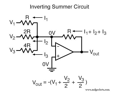
The R/2nR DAC—often called a binary‑weighted input DAC—is a specialized form of the inverting summing amplifier. It converts a set of binary input voltages into a single analog voltage whose magnitude is proportional to the binary number represented.
In a standard inverting summing op‑amp, all input resistors are equal so that each input contributes equally to the output. The R/2nR design intentionally assigns resistors that follow a power‑of‑two series (R, 2R, 4R, …), giving each successive bit half the influence of the one before it.
This weighting aligns with the place values of binary digits, allowing the circuit to produce an analog voltage that is a faithful linear representation of the digital input.
Illustrative Example
Consider a three‑bit DAC with input resistors set to R, 2R, and 4R, as shown:
Driving each input with a logic level (0 V or the supply voltage) yields the following output voltage sequence:
-------------- | Binary | Output voltage |
-------------- | 000     | 0.00 V |
-------------- | 001     | -1.25 V |
-------------- | 010     | -2.50 V |
-------------- | 011     | -3.75 V |
-------------- | 100     | -5.00 V |
-------------- | 101     | -6.25 V |
-------------- | 110     | -7.50 V |
-------------- | 111     | -8.75 V |
Each increment in the binary count produces a 1.25 V step in the output. The sign is negative because the op‑amp is configured inverting.
Simulating the Circuit
The design can be verified with a simple SPICE simulation. For a binary input of 110 (where the first input node is tied to the positive supply and the second to ground), the netlist is:
binary-weighted dac v1 1 0 dc 5 rbogus 1 0 99k r1 1 5 1k r2 1 5 2k r3 0 5 4k rfeedbk 5 6 1k e1 6 0 5 0 999k .end
node voltage node voltage node voltage (1) 5.0000 (5) 0.0000 (6) -7.5000
The simulated output appears on node 6, matching the expected –7.50 V for the binary code 110.
Adjusting the Output Range
By changing the feedback resistor value, the DAC’s output voltage range can be scaled. For example, using an 800 Ω feedback resistor instead of 1 kΩ yields:
Binary | Output voltage
-------|----------------
000    | 0.00 V
001    | -1.00 V
010    | -2.00 V
011    | -3.00 V
100    | -4.00 V
101    | -5.00 V
110    | -6.00 V
111    | -7.00 V
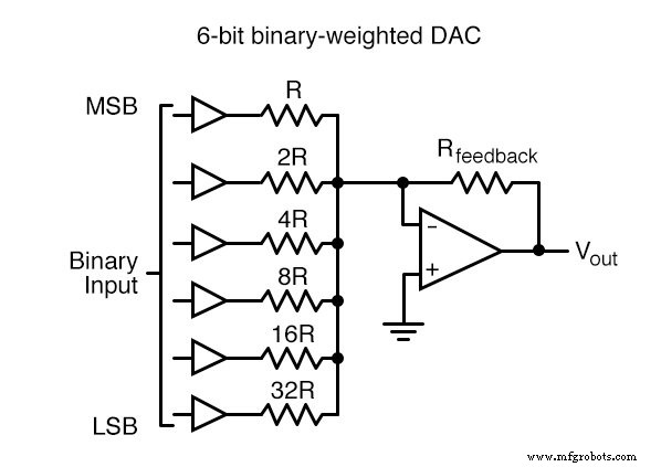
Scaling to Higher Resolution
Adding more bits is straightforward: insert additional input resistors following the 2ⁿ sequence. The circuit diagram for a four‑bit DAC is:
Practical Design Considerations
- All digital drivers must supply identical high and low voltage levels (e.g., +5 V high, 0 V low). Variations degrade the analog accuracy.
- Using CMOS logic gates minimizes the current required from each driver, preserving the resistor ratio integrity.
- Choosing resistor values that limit driver current reduces power consumption and heat.
- For high‑resolution applications, consider the op‑amp’s offset voltage and bias current; these can introduce small but measurable errors.
When to Use an R/2nR DAC
Binary‑weighted DACs are ideal for low‑to‑moderate resolution (up to about 8–10 bits) in audio, instrumentation, and control systems where simplicity and cost are critical. For higher resolutions, switched‑capacitor or sigma‑delta DACs are typically preferred due to their superior linearity and tolerance to component variations.
Industrial Technology
- The 555 Integrated Circuit: A Timeless Benchmark in Analog Design
- The Quadratic Formula: A Reliable Tool for Solving Second‑Degree Equations
- Mastering the D Latch: A Clean 1‑Bit Memory Circuit
- Understanding the R/2R Ladder Digital‑to‑Analog Converter
- Common‑Base Transistor Amplifiers: Design, Analysis, and Applications
- DIAC: The Bidirectional Trigger for AC Thyristors
- Choosing the Right Video Converter: A Guide to Selecting the Best Software
- AC-DC Converters: Your Reliable Source for Consistent DC Power
- Build a High‑Quality DIY Digital‑Analog Converter: Complete Step‑by‑Step Guide
- Digital-to-Analog Converters (DACs): Key Types and Their Applications