


Early Nonmechanical Memory Technologies: From Delay Lines to Core Memory
In the formative years of computing, designers pushed beyond mechanical relays and vacuum tubes, pioneering nonmechanical storage solutions that would shape modern memory architecture.
One of the most inventive concepts was the delay line. A delay line delays the propagation of a pulse or wave—much like an echo bouncing through a canyon. By converting electrical impulses into acoustic waves in a medium such as mercury, and then reconverting them back, the line temporarily “stores” data as the waves circulate.
Early implementations used long tubes filled with liquid mercury. An electrical transducer at each end converted signals to sound waves and back. A serial stream of binary data entered the transmitting transducer as a voltage waveform, traveled through the mercury, and emerged from the receiving transducer in the same order.
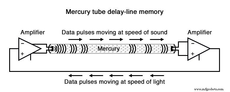
When a feedback circuit repeatedly drove the transmitting transducer, the sequence of pulses became a circulating FIFO shift register—effectively a ring counter that could retain data as long as the loop remained powered.
Despite its ingenuity, the delay line suffered from material and environmental constraints. The EDVAC in the early 1950s employed 128 mercury tubes, each roughly 5 ft long, holding a maximum of 384 bits. Temperature shifts altered the speed of sound in mercury, skewing timing and compromising reliability.
Subsequent designs replaced liquid mercury with solid rods—glass, quartz, or specially alloyed metal—to delay torsional waves at higher frequencies. A notable example used a 95‑ft long nickel‑iron‑titanium wire, coiled for compactness. The total delay was 9.8 ms, enabling a 1 MHz clock and roughly 9,800 bits of storage per wire.
Although delay lines eventually gave way to more robust technologies, the principle of using physical media to hold data remains foundational in modern memory research.
Another milestone was the Williams Tube, a cathode‑ray tube (CRT) adapted from oscilloscope and television displays. Instead of exciting phosphor to create an image, the electron beam deposited charge on the glass surface. A metal grid positioned in front of the tube detected this charge, and external circuitry refreshed the data to prevent loss.
IBM’s Model 701 employed a Williams Tube memory with 4 kB capacity. However, repeated rewrites could over‑charge the screen, causing stray “1” states to bleed into neighboring pixels.
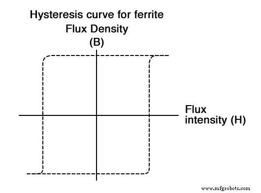
Magnetic core memory represented a decisive leap forward. Ferromagnetic ferrite compounds exhibit a nearly square hysteresis curve: a critical magnetic field threshold is required to flip the magnetization direction, and once flipped, the material retains its state even when the field is removed. This bistability makes ferrite ideal for a binary latch.
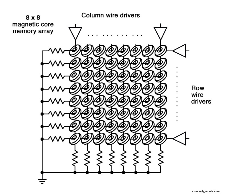
Jay Forrester of MIT harnessed this property to build the first practical core memory. A grid of insulated wires crossed through thousands of ferrite rings—each ring being a core. By energizing the row and column wires that intersect at a core, a magnetic field strong enough to set or reset the core’s polarity is generated. The direction of the applied current determines whether the core stores a “0” or a “1.”
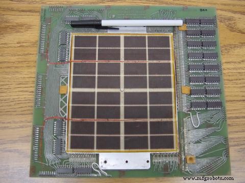
Data General’s Nova computer, circa 1969–70, housed a 4 kB core memory board. The cores were barely larger than a ball‑point pen, and the board’s circuitry drove the row/column currents and read the core states.
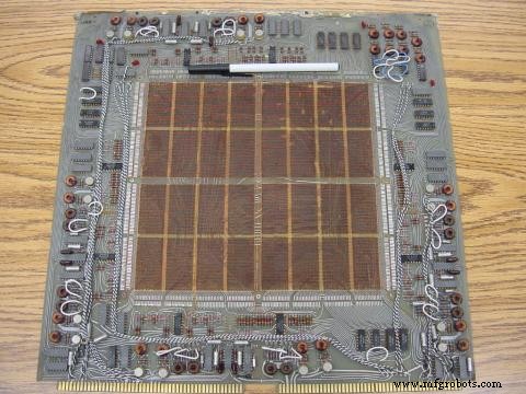
A later 1971 design packed cores more densely, doubling capacity to 8 kB.
Reading a core was a destructive process: a voltage pulse written to the core would induce a current on a dedicated read wire only if the core’s state changed. Consequently, the core had to be written again to preserve its original value, necessitating periodic refresh cycles.
Core memory’s strengths were nonvolatility, ruggedness, and relatively high density—all achieved without the mechanical wear of delay lines or the temperature sensitivity of CRTs. These attributes made core memory the backbone of many 1960s–70s systems, including Apollo guidance computers, CNC controllers, and business mainframes.
Meanwhile, static RAM (SRAM) evolved in parallel, driven by smaller transistors and eventually silicon ICs. SRAM’s nonvolatile advantage kept it alive, but the scale and cost of core memory ultimately edged it out by the 1980s.
Bubble memory offered another magnetic alternative. In a thin garnet film under a permanent magnetic field, micron‑sized magnetized “bubbles” could be slid along etched tracks using external coils. A bubble represented a “1,” and its absence a “0.” Reading and writing occurred as bubbles passed a tiny detection coil, akin to a tape head.
Despite its impressive density—millions of bits on a chip only a few square inches in size—bubble memory suffered from inherently sequential access, limiting performance relative to dynamic and static RAM.
An electrostatic cousin, the Charge‑Coupled Device (CCD), moved electrical charges across a silicon substrate in a similar serial fashion. Like bubble memory, CCDs required frequent refresh due to charge decay, rendering them volatile.
In summary, the progression from delay lines to core memory illustrates the relentless drive to increase storage density, reliability, and speed—principles that continue to inform today’s memory technologies.
Industrial Technology
- Understanding Non‑Mechanical Digital Memories: SRAM, DRAM, and Flash
- Understanding ROM, PROM, EPROM, and EEPROM: Design, Programming, and Identification
- From Punched Cards to Hard Drives: The Evolution of Mechanical Storage
- Understanding Look‑Up Tables: From ROMs to Advanced ALUs
- Microprocessors: The Evolution of Stored‑Program Computing
- Understanding Junction Diodes: From Crystal Detectors to Modern Silicon Devices
- Exploring Advanced Diode Technologies: Varicaps, PINs, IMPATT, Gunn, and More
- Advanced Cockpit Displays: The F/A‑18 Super Hornet’s Touchscreen Innovation
- Lightfastness of Dyes: James Morton’s Pioneering Legacy in Textile Color Durability
- Protect Your Business: Safeguard Against Ransomware Attacks