


Implementing an AXI FIFO in Block RAM Using Ready/Valid Handshake
When I first encountered the AXI interface while designing a module, I was surprised by its streamlined flow‑control approach. Unlike traditional protocols that rely on busy/valid, full/valid, or empty/valid pairs, AXI uses only two signals: ready and valid. What began as frustration quickly became fascination.
AXI embeds flow control directly into its handshake, eliminating the need for extra status lines. While the basic rules are straightforward, careful attention is required when mapping the protocol to FPGA hardware. In this tutorial, I walk through a VHDL implementation of an AXI FIFO that runs on block RAM.
AXI solves the delayed‑by‑one‑cycle problem
Preventing over‑read and overwrite is a common challenge when two clock‑synchronised modules exchange data streams. The crux of the issue is that each module can only observe the other’s output one clock cycle after it occurs.

The diagram above illustrates a sequential module writing to a FIFO that uses the classic write enable/full signalling scheme. The writer asserts wr_en to push data into the FIFO, while the FIFO raises full when no more space is available. The problem is that full is asserted exactly on the rising edge of the clock, so the writer can no longer react to it in the same cycle. The solution is to provide a look‑ahead signal such as almost_empty, giving the upstream logic a head start.
The ready/valid handshake
AXI stream interfaces solve this timing dilemma with a two‑signal handshake: ready and valid. The receiver drives ready; a high value indicates that it is prepared to accept a new datum. The sender drives valid; a high value means the data on the bus is stable and can be sampled. A transfer occurs only when both signals are high on the same rising edge.

The waveform demonstrates a single data item transfer. Data is sampled on the rising clock edge, just as in conventional synchronous designs.
Implementation
There are several ways to build an AXI FIFO in VHDL. While a shift register would work, a ring buffer backed by block RAM is the most efficient and scalable choice. Below, I present a modular design that separates the logic into dedicated processes for clarity and synthesiser friendliness.
The entity
The entity defines two generic parameters – ram_width and ram_depth – that set the word width and the FIFO depth. The capacity is effectively ram_depth - 1, because one slot is reserved to differentiate a full FIFO from an empty one.
entity axi_fifo is
  generic (
    ram_width : natural;
    ram_depth : natural
  );
  port (
    clk : in std_logic;
    rst : in std_logic;

    -- AXI input interface
    in_ready : out std_logic;
    in_valid : in std_logic;
    in_data : in std_logic_vector(ram_width - 1 downto 0);

    -- AXI output interface
    out_ready : in std_logic;
    out_valid : out std_logic;
    out_data : out std_logic_vector(ram_width - 1 downto 0)
  );
end axi_fifo;
The interface follows AXI conventions: the input side uses in_ready and in_valid, while the output side mirrors the signals with reversed directions. This symmetry allows multiple FIFOs to be chained seamlessly.
Signal declarations
First, we define a RAM type that matches the generic width and depth, then we instantiate the array:
-- The FIFO is full when the RAM contains ram_depth - 1 elements
  type ram_type is array (0 to ram_depth - 1)
    of std_logic_vector(in_data'range);
  signal ram : ram_type;
Next, we declare an index subtype that can represent any address in the RAM, and four core signals: head, tail, count, and a delayed copy count_p1:
subtype index_type is natural range ram_type'range;
  signal head : index_type;
  signal tail : index_type;
  signal count : index_type;
  signal count_p1 : index_type;
We also keep internal versions of the ready and valid outputs to avoid reading out signals inside the architecture:
signal in_ready_i : std_logic;
  signal out_valid_i : std_logic;
A helper signal tracks when a simultaneous read and write occurs in the previous cycle, which is critical for correctly setting out_valid when the FIFO is almost empty:
signal read_while_write_p1 : std_logic;
Subprograms
The next_index function determines the next address based on whether a read or write handshake just completed. It wraps around when the end of the array is reached.
function next_index(
  index : index_type;
  ready : std_logic;
  valid : std_logic) return index_type is
begin
  if ready = '1' and valid = '1' then
    if index = index_type'high then
      return index_type'low;
    else
      return index + 1;
    end if;
  end if;

  return index;
end function;
The index_proc procedure encapsulates the synchronous logic that updates either the head or tail pointer. This avoids duplicate code and keeps the architecture tidy.
procedure index_proc(
  signal clk : in std_logic;
  signal rst : in std_logic;
  signal index : inout index_type;
  signal ready : in std_logic;
  signal valid : in std_logic) is
begin
    if rising_edge(clk) then
      if rst = '1' then
        index <= index_type'low;
      else
        index <= next_index(index, ready, valid);
      end if;
    end if;
end procedure;
Copy internal signals to the output
in_ready <= in_ready_i;
  out_valid <= out_valid_i;
Update the head and tail
We instantiate the helper procedure twice – once for the write pointer (head) and once for the read pointer (tail):
PROC_HEAD : index_proc(clk, rst, head, in_ready_i, in_valid);
  PROC_TAIL : index_proc(clk, rst, tail, out_ready, out_valid_i);
Infer block RAM
Block RAM in most FPGAs is synchronous. To let the synthesiser infer a RAM primitive, we keep the read and write operations inside a clocked process and avoid explicit enable signals:
PROC_RAM : process(clk)
begin
  if rising_edge(clk) then
    ram(head) <= in_data;
    out_data <= ram(next_index(tail, out_ready, out_valid_i));
  end if;
end process;
The write occurs unconditionally on the cycle when in_valid is high, and the read data is updated every cycle so that the consumer can observe a valid word whenever the FIFO contains data.
Count the number of elements in the FIFO
The count signal reflects the current occupancy. When head is ahead of tail, the count is simply the difference; if the head has wrapped, we add the total depth:
PROC_COUNT : process(head, tail)
begin
  if head < tail then
    count <= head - tail + ram_depth;
  else
    count <= head - tail;
  end if;
end process;
The delayed copy count_p1 is needed to detect when the FIFO was empty in the previous cycle, which influences out_valid:
PROC_COUNT_P1 : process(clk)
begin
  if rising_edge(clk) then
    if rst = '1' then
      count_p1 <= 0;
    else
      count_p1 <= count;
    end if;
  end if;
end process;
Update the ready output
The writer should be told when the FIFO can accept more data. The ready signal is high whenever the count is less than ram_depth - 1:
PROC_IN_READY : process(count)
begin
  if count < ram_depth - 1 then
    in_ready_i <= '1';
  else
    in_ready_i <= '0';
  end if;
end process;
Detect simultaneous read and write
When both a read and a write occur in the same cycle, the FIFO does not change its occupancy but the internal state must reflect that a value will become available only after two cycles when the FIFO is almost empty. We therefore capture this event in read_while_write_p1:
PROC_READ_WHILE_WRITE_P1: process(clk)
begin
  if rising_edge(clk) then
    if rst = '1' then
      read_while_write_p1 <= '0';
    else
      read_while_write_p1 <= '0';
      if in_ready_i = '1' and in_valid = '1' and
        out_ready = '1' and out_valid_i = '1' then
        read_while_write_p1 <= '1';
      end if;
    end if;
  end if;
end process;
Update the valid output
The out_valid signal tells downstream logic when out_data holds a usable word. The combinational process below sets it high by default but clears it in two corner cases:
PROC_OUT_VALID : process(count, count_p1, read_while_write_p1)
begin
  out_valid_i <= '1';

  -- If the FIFO is empty or was empty in the previous cycle
  if count = 0 or count_p1 = 0 then
    out_valid_i <= '0';
  end if;

  -- If a simultaneous read/write occurred when the FIFO had only one item
  if count = 1 and read_while_write_p1 = '1' then
    out_valid_i <= '0';
  end if;

end process;
The first condition guarantees that out_valid remains low during the propagation delay after the first write. The second guards against a situation where the FIFO appears to stay full for one cycle but actually holds no data to output.
Synthesising in Vivado
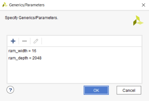
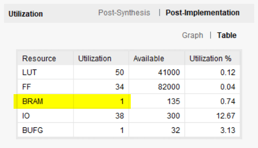
To synthesize this design in Xilinx Vivado, supply concrete values for the generics. In the Settings dialog (General → Generics/Parameters), choose a depth that matches a RAMB36E1 primitive for the target Zynq device. After implementation, the resource utilisation is modest – one block RAM plus a handful of LUTs and FFs.
AXI is more than ready/valid
AXI (Advanced eXtensible Interface) is a component of ARM’s AMBA bus architecture and offers a rich feature set beyond the simple ready/valid handshake. For deeper understanding, consider the following resources:
- Wikipedia: AXI
- ARM AXI introduction
- Xilinx AXI introduction
- AXI4 specification
VHDL
- The Cloud Revolution: How Cloud Computing Transforms IT, Security, and Careers
- Unlocking IoT Data: How Business Rules Management Drives Enterprise Value
- Creating a Breathing LED Effect Using a Sine Wave from Block RAM
- Initializing FPGA Block RAM from Text Files Using VHDL’s TEXTIO Library
- Preparing Your Manufacturing Operations for AI with IoT
- Harness CMMS Data: Build Insightful Dashboards & Reports for Smart Decisions
- Asset Tracking Best Practices: Unlocking the Value of Your Asset Data
- Ensuring Trustworthy Supply‑Chain Data: A Proven Strategy
- Optimize Your Maintenance Supply Chain with Data-Driven Automation
- 3D Printing a Protective Mask: A Step-by-Step Guide