

Industrial manufacturing
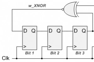
LFSR in an FPGA – VHDL & Verilog Code How a Linear Feedback Shift Register works inside of an FPGA LFSR stands for Linear Feedback Shift Register and it is a design that is useful inside of FPGAs. LFSRs are simple to synthesize, meaning that they take relatively few resources and can be run at v
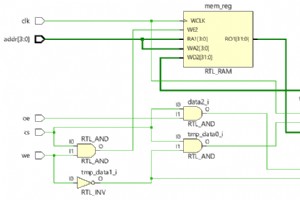
Design module single_port_sync_ram # (parameter ADDR_WIDTH = 4, parameter DATA_WIDTH = 32, parameter DEPTH = 16 ) ( input clk, input [ADDR_WIDTH-1:0] addr, inout [DATA_WIDTH-1:0] data, input cs, input we, input oe ); reg
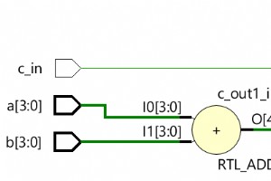
An adder is a digital component that performs addition of two numbers. Its the main component inside an ALU of a processor and is used to increment addresses, table indices, buffer pointers and in a lot of other places where addition is required.A full adder adds a carry input along with other input
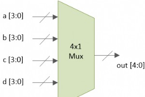
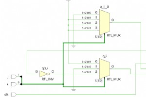
What is a mux or multiplexer ?A multiplexer or mux in short, is a digital element that transfers data from one of the N inputs to the output based on the select signal. The case shown below is when N equals 4. For example, a 4 bit multiplexer would have N inputs each of 4 bits where each input can b
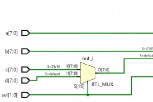
Design module pr_en ( input [7:0] a, input [7:0] b, input [7:0] c, input [7:0] d, input [1:0] sel, output reg [7:0] out); always @ (a or b or c or d or sel) begin if (sel == 2b00) out <= a; else i
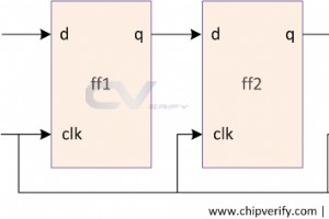
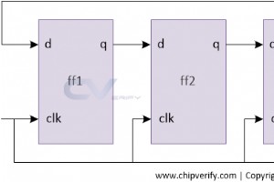
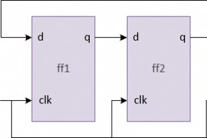
In digital electronics, a shift register is a cascade of flip-flops where the output pin q of one flop is connected to the data input pin (d) of the next. Because all flops work on the same clock, the bit array stored in the shift register will shift by one position. For example, if a 5-bit right sh

Design module gray_ctr # (parameter N = 4) ( input clk, input rstn, output reg [N-1:0] out); reg [N-1:0] q; always @ (posedge clk) begin if (!rstn) begin q <= 0; out <= 0; end else begin q <= q + 1; `ifdef FOR_LOOP for (int i
Design module modN_ctr # (parameter N = 10, parameter WIDTH = 4) ( input clk, input rstn, output reg[WIDTH-1:0] out); always @ (posedge clk) begin if (!rstn) begin out <= 0; end else begin if (out == N-1) out <= 0; else out
Design module johnson_ctr #(parameter WIDTH=4) ( input clk, input rstn, output reg [WIDTH-1:0] out ); always @ (posedge clk) begin if (!rstn) out <= 1; else begin out[WIDTH-1] <= ~out[0]; for (int i = 0; i < WIDTH-1; i=i+1)
Design module ring_ctr #(parameter WIDTH=4) ( input clk, input rstn, output reg [WIDTH-1:0] out ); always @ (posedge clk) begin if (!rstn) out <= 1; else begin out[WIDTH-1] <= out[0]; for (int i = 0; i < WIDTH-1; i=i+1) be
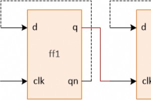
A ripple counter is an asynchronous counter in which the all the flops except the first are clocked by the output of the preceding flop. Design module dff ( input d, input clk, input rstn, output reg q, output qn); always @ (pose
The 4-bit counter starts incrementing from 4b0000 to 4h1111 and then rolls over back to 4b0000. It will keep counting as long as it is provided with a running clock and reset is held high.The rollover happens when the most significant bit of the final addition gets discarded. When counter is at a ma
A flip-flop captures data at its input at the positive or negative edge of a clock. The important thing to note is that whatever happens to data after the clock edge until the next clock edge will not be reflected in the output. A latch on the other hand, does not capture at the edge of a clock, ins
Design module tff ( input clk, input rstn, input t, output reg q); always @ (posedge clk) begin if (!rstn) q <= 0; else if (t) q <= ~q; else q <= q; end endmodule Testbench module tb; reg clk; reg rs
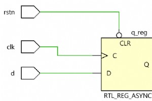
A D flip-flop is a sequential element that follows the input pin d at the given edge of a clock.Design #1: With async active-low reset module dff ( input d, input rstn, input clk, output reg q); always @ (posedge clk or negedge rstn) if (!rst
Design module jk_ff ( input j, input k, input clk, output q); reg q; always @ (posedge clk) case ({j,k}) 2b00 : q <= q; 2b01 : q <= 0; 2b10 : q <= 1; 2b11 : q <= ~q; endcase endmodule Hardw
Its always best to get started using a very simple example, and none serves the purpose best other than Hello World !. // Single line comments start with double forward slash // // Verilog code is always written inside modules, and each module represents a digital block with some functionality m
Verilog has system tasks and functions that can open files, output values into files, read values from files and load into other variables and close files.Opening and closing files module tb; // Declare a variable to store the file handler integer fd; initial begin // Open a new file by t
Default timescaleAlthough Verilog modules are expected to have a timescale defined before the module, simulators may insert a default timescale. The actual timescale that gets applied at any scope in a Verilog elaborated hierarchy can be printed using the system task $printtimescale which accepts th
Verilog timescale directive specifies time unit and precision for simulations.Verilog $timeformat system function specifies %t format specifier reporting style in display statements like $display and $strobe.Syntax $timeformat(<unit_number>, <precision>, <suffix_string>, <mi
Verilog

Molybdenum Recovery and Utilization: Current Trends and Techniques
Mastering Lean Manufacturing: 5S, Kaizen, and Continuous Improvement

Holistic Design: A Comprehensive, Sustainable Approach to System Creation

Superior Performance of Inverted Perovskite Solar Cells Using CdSe Quantum Dot and LiF Electron Transport Layers

