


Cross‑Sectional KPFM Reveals Potential Dip and Schottky Barrier in Thick PCDTBT:PCBM Bulk Heterojunction Solar Cells
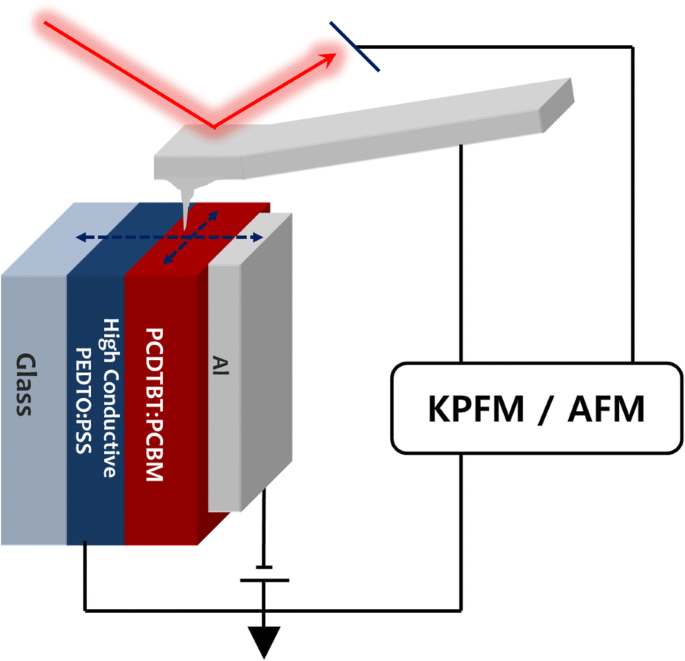
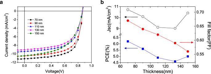
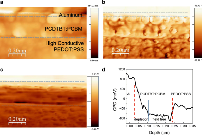
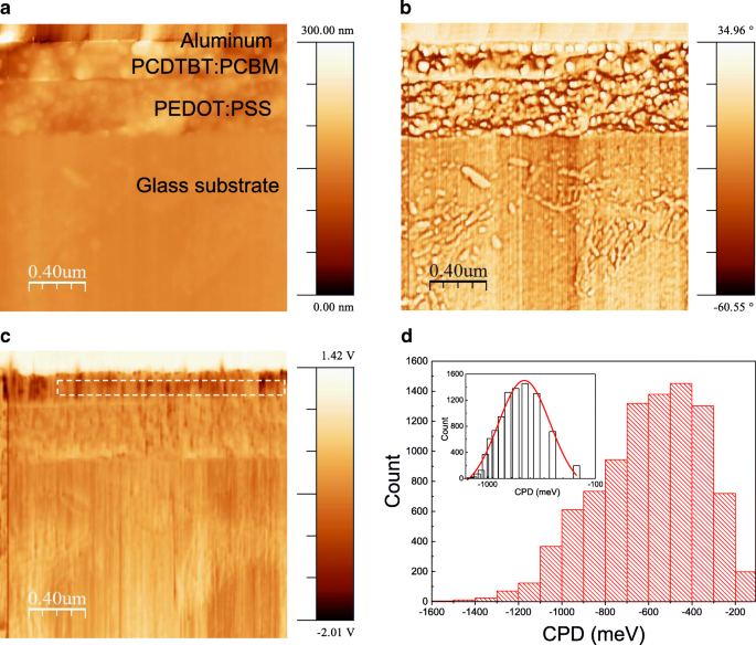
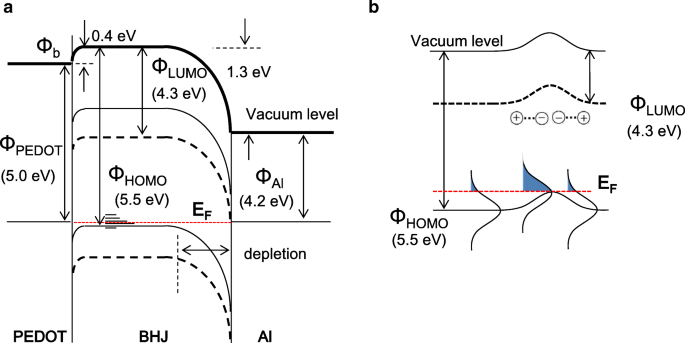
Kelvin probe force microscopy (KPFM) was used to map the cross‑sectional potential distribution of a high‑open‑circuit‑voltage PCDTBT:PCBM bulk heterojunction (BHJ) solar cell. The potential drop is confined to the cathode interface, confirming the p‑type behaviour of the photo‑active layer. In the field‑free central region the measured potentials follow a log‑normal distribution, indicating a broad energetic disorder that can trap holes and enhance bimolecular recombination. A Schottky barrier at the anode interface further impedes charge extraction, while the potential gradient in the depletion region can mitigate the dip by lowering the barrier for trapped carriers. Organic photovoltaics (OPVs) promise low‑cost, flexible solar solutions, yet their commercial viability hinges on power‑conversion efficiencies (PCEs) above 10 %. Recent progress has been driven by novel donor/acceptor materials and optimized fabrication protocols. The classic P3HT:PCBM pair achieved 3–5 % PCE, but thicker active layers, necessary for higher light absorption, suffer from reduced charge‑collection efficiency due to increased recombination and energetic disorder. Cross‑sectional KPFM offers nanoscale insight into internal electric fields and potential landscapes, yet most studies have focused on the P3HT:PCBM system. Here we extend this approach to the PCDTBT:PCBM BHJ, a material that exhibits near‑unity internal quantum efficiency in thin devices but suffers from performance loss in thicker films. PCDTBT (donor) and soluble PCBM (acceptor) were spin‑coated to form active layers 70–150 nm thick on a 20 nm PEDOT:PSS hole‑transport layer (HTL) atop ITO. Aluminum cathodes were evaporated under high vacuum. For KPFM, a 200 nm active layer on a highly conductive PEDOT:PSS anode was cleaved in liquid nitrogen to expose a smooth cross‑section. J–V curves were recorded with a Keithley 236 under AM 1.5G illumination (100 mW cm⁻²). KPFM (n‑Tracer Nanofocus) was performed in dry nitrogen; AFM topography and frequency‑modulated CPD were simultaneously acquired using a Pt/Ir‑coated cantilever (350 kHz). Increasing the active‑layer thickness shifts the short‑circuit current (J_SC) due to interference effects, while the open‑circuit voltage (V_OC) remains constant, indicating unchanged built‑in potential. However, the fill factor (FF) steadily decreases with thickness, reflecting poorer charge collection. The KPFM topography (Fig. 3a) shows a smooth cleaved surface with <200 nm RMS roughness. Phase imaging (Fig. 3b) delineates the PEDOT:PSS/PCDTBT:PCBM interface. CPD mapping (Fig. 3c) reveals a steep potential drop confined to the cathode side (≈70 nm), characteristic of the depletion region. The mid‑region near the anode is field‑free, confirming the BHJ behaves as an effective p‑type semiconductor. A pronounced potential dip appears near the anode interface (Fig. 3c). To confirm its spatial extent, a larger area was imaged (Fig. 4). The CPD image shows random bright and dark spots across the BHJ, indicating a wide energetic disorder that follows a log‑normal distribution (Fig. 4d). The long tail of the distribution (σ ≈ 400 meV) suggests a high density of deep trap states, which can capture holes and increase bimolecular recombination. The measured potentials translate into an energy band diagram (Fig. 5a) where the PEDOT:PSS anode forms a 0.4 eV Schottky barrier with the deep HOMO of PCDTBT. This barrier lengthens hole residence time, raising the likelihood of recombination. The potential dip in the field‑free region (Fig. 5b) is a manifestation of dipole‑induced band bending caused by the distribution of hole traps. If the active layer were thinner (≈70 nm), the depletion field would overlap the dip, effectively lowering the Schottky barrier (Schottky‑barrier lowering) and facilitating charge extraction. Replacing PEDOT:PSS with a deeper‑workfunction HTL such as MoOx would convert the anode junction into an ohmic contact, further improving extraction efficiency. Nonetheless, the intrinsic energetic disorder remains a bottleneck for thick devices, underscoring the importance of thin, high‑quality active layers or advanced interfacial engineering. Cross‑sectional KPFM of thick PCDTBT:PCBM BHJ cells revealed a Schottky barrier at the anode and a log‑normal distributed potential dip in the field‑free region. These features trap holes and enhance bimolecular recombination, explaining the observed drop in fill factor for thicker films. Mitigation strategies include using deeper‑workfunction HTLs to eliminate the Schottky barrier and designing devices with active‑layer thicknesses comparable to the depletion width to suppress the potential dip via Schottky‑barrier lowering.Abstract
Background
Methods
Materials and Device Fabrication
Electrical and KPFM Characterization
Results and Discussion
Thickness‑Dependent Photovoltaic Performance
Cross‑Sectional Potential Mapping
Energy Band Diagram and Implications
Conclusions
Abbreviations
Nanomaterials
- IBM Breaks New Ground: First Liquid‑Phase Atomic Imaging of 2D Materials at Room Temperature
- High‑Efficiency, Excitation‑Independent Blue‑Emitting Carbon Dots with Tunable Photoluminescence
- Impact of Sulfate Anions on Ultrafine Titania Nucleation During TiCl4 Hydrolysis
- Atomic Force Microscopy of Glass Transition and Adhesion in Thin Polystyrene Films
- High-Performance Wavelength-Selective Photodetector Using a Single CdSSe Nanobelt
- Low-Temperature Annealing of Graphene Oxide Films: Impact on Electrical Conductivity and Surface Potential via SKPFM
- How Temperature Influences the Young’s Modulus of Electrospun Polyurethane Nanofibers
- Measuring Local Open‑Circuit Voltage in Si Nanowire Radial Junctions Using Kelvin Probe Force Microscopy
- Nano-Clays: A Promising Nano-Immune Defense Against COVID-19
- Quantitative Nanomechanical Mapping of LDPE Elastomers Using Atomic Force Microscopy