


Nanoclusters Enable Magnetic Plasmon Waveguides Beyond the Diffraction Limit
 Focusing light at the nanoscale
Conventional optics limit the smallest focus to roughly half the wavelength of light. Recent advances in nanoplasmonics have shattered this barrier by coupling light to surface plasmon resonances in engineered metallic nanostructures, allowing sub‑wavelength confinement and manipulation of optical fields.
Plasmonic waveguidesSurface plasmons arise when conduction electrons in a metal oscillate coherently along its surface. When these oscillations follow a circular path, they generate magnetic plasmons—analogous to magnetic dipoles—that can propagate with minimal losses. Magnetic plasmonic waveguides excel in miniaturization, outperforming electronic counterparts and enabling light guidance far below the diffraction limit.
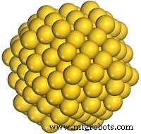
Fused heptamer waveguidesResearchers at Rice University have fabricated magnetic plasmonic waveguides composed of fused heptamers—artificial ring‑like molecules that host circulating currents when illuminated at 1500 nm. Each heptamer pair shares two gold nanoparticles, forming a robust inter‑molecular link that facilitates efficient current transfer and supports micron‑scale propagation along a conjugated chain.
Wave‑guiding networksBuilding on the fused heptamer platform, the team demonstrated complex routing devices: a steerer that bends plasmonic signals through large angles, and a Y‑splitter that divides and recombines plasmonic waves. The Y‑splitter can also act as an interferometric switch, enabling on‑off control of plasmon propagation.
ApplicationsThese nanostructures provide a blueprint for next‑generation photonic components, promising low‑loss energy transport, high‑density data storage, and enhanced near‑field microscopy. Tailored metallic nanostructures may also pave the way for compact optoelectronic devices operating at the nanoscale.
Nanomaterials
- Understanding Relay Construction: From Solenoids to Industrial Applications
- Electromagnetism: From Oersted’s Discovery to Modern Applications
- The Evolution of Videotape: Revolutionizing Media & Home Entertainment
- Magnets: Types, Materials, Manufacturing, and Future Applications
- The Evolution of Floppy Disks: From Magnetic Media to Optical Storage
- Types of Magnetometers: From Scalar to Advanced Vibrating‑Sample Devices
- Nanodiamonds: Ultra‑Precise Magnetic Sensors for Biomedical and Quantum Applications
- Impact of Magneto‑Dipole Interactions on the Specific Absorption Rate of Iron Oxide Nanoparticle Assemblies
- Revolutionizing Brain Imaging: The Wearable Metamaterial Explained
- Understanding Magnetic Clutches: Function, Design, and Applications