


Understanding Clipper Circuits: Theory, Simulation, and Practical Applications
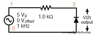
A clipper is a passive electronic circuit that limits a waveform’s peak amplitude. The following analysis focuses on a negative‑clipper configuration, illustrating how a single diode and resistor restrict the signal below a set voltage threshold.
Clapper Circuit Operation Analysis
The schematic was generated using the Xcircuit capture tool, and the accompanying SPICE netlist was exported automatically. Minor edits were made to the netlist using a text editor to insert the diode component.
*SPICE 03437.eps
* A K ModelName D1 0 2 diode R1 2 1 1.0k V1 1 0 SIN(0 5 1k)
.model diode d
.tran .05m 3m
.end
Clipper: clips negative peak at –0.7 V.
Positive Half Cycle
When the input sine wave rises to its positive peak (5 V), the diode is reverse‑biased and remains non‑conductive. The output at node 2 simply mirrors the input during this half‑cycle, as shown in the simulation. For display clarity, the simulator’s “plot v(1)+1” command offsets the input waveform by 1 V.
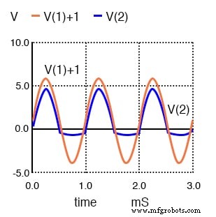
In the plot, V(1)+1 is actually the 10 V peak‑to‑peak sine wave, shifted upward. The output V(2) is clipped at –0.7 V by diode D1.
Negative Half Cycle
During the negative portion of the sine wave, the diode becomes forward‑biased and conducts. The input is effectively shorted to ground, causing the output to follow the input only until it reaches the diode’s forward‑drop threshold. For a silicon diode, the default forward voltage is 0.7 V unless the model is parameterized otherwise. Germanium or Schottky diodes will clip at lower voltages, which can be verified against their datasheets.
The simulation shows that the clipping occurs only after the input exceeds –0.7 V; the diode does not conduct throughout the entire negative half‑cycle.
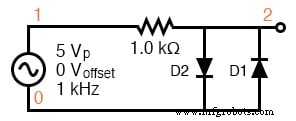
Symmetrical Clipper Circuit
Adding an anti‑parallel diode to the existing configuration yields a symmetrical clipper that limits both positive and negative peaks. The following netlist reflects this change:
*SPICE 03438.eps
D1 0 2 diode
D2 2 0 diode
R1 2 1 1.0k
V1 1 0 SIN(0 5 1k)
.model diode d
.tran 0.05m 3m
.end
Symmetrical clipper: Anti‑parallel diodes clip both positive and negative peaks, producing a ±0.7 V output.
Diode D1 clamps the negative half‑cycle at –0.7 V, while D2 conducts during the positive half‑cycle once the input surpasses +0.7 V. The remaining voltage is dropped across the series resistor, ensuring that the output never exceeds ±0.7 V.
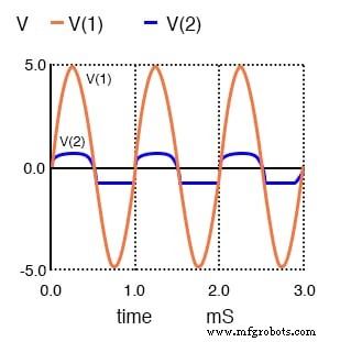
Simulation confirms the expected clipping behavior for both diodes.
General Form of the Diode Clipper
The most versatile diode clipper design incorporates adjustable voltage references to set precise clipping levels. For a real silicon diode, the forward‑drop must be accounted for in the reference voltages. In the example below, D1 begins conducting at 1.3 V + 0.7 V = 2.0 V, and D2 at –2.3 V – 0.7 V = –3.0 V.
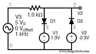
*SPICE 03439.eps
V1 3 0 1.3
V2 4 0 -2.3
D1 2 3 diode
D2 4 2 diode
R1 2 1 1.0k
V3 1 0 SIN(0 5 1k)
.model diode d
.tran 0.05m 3m
.end
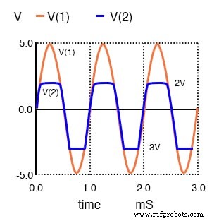
D1 clips the input at 2 V; D2 clips at –3 V.
To clip only one side, simply remove the corresponding diode and voltage source. The following simulation demonstrates a clipper that limits the positive half‑cycle to 2 V while allowing the negative half‑cycle to pass unaltered.
Zener Diode Clipper
A Zener diode can replace both the clipping diode and the DC reference voltage, providing a self‑biased clipping level determined by the Zener breakdown voltage. This configuration is especially useful in high‑voltage applications where precise clipping is required.
Practical Application of Clipper Circuits
Clipper circuits serve as critical protection devices in many electronic systems. For instance, when amplifying voice signals before feeding them into a radio transmitter, a clipper prevents the amplified signal from exceeding the transmitter’s linear range. Over‑driving the transmitter not only distorts the output but also generates spurious emissions that can interfere with adjacent stations.
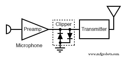
The clipper in the figure protects the transmitter by limiting peak voltage excursions caused by loud speech.
Other common applications include:
- Converting a sine wave into a square wave by deliberately over‑driving a clipper.
- Protecting the input stages of integrated circuits. In a CMOS IC, the clipper diodes reference the 0 V and +5 V rails, clamping the input to the device’s safe operating range.
- Using a resistor–diode pair with a DC bias to clip at an arbitrary voltage level, a technique employed in level‑shifting and signal conditioning.
Review
- Resistor–diode pairs clip the signal at a predetermined voltage.
- Anti‑parallel Si diodes provide symmetrical clipping at ±0.7 V.
- Grounded diode terminals can be replaced with a DC bias to set arbitrary clipping thresholds.
- Clipper circuits act as protective elements, preventing signals from exceeding specified limits.
Related Worksheets:
- Clipper and Clamper Circuits Worksheet
Industrial Technology
- Foundations of DC Circuits: Understanding Direct Current and Core Electrical Concepts
- Understanding AC Circuits: A Beginner's Guide
- Commutating Diode Experiment: Suppressing Inductive Kickback with a Neon Lamp
- Voltage Regulator Experiment with a 12‑Volt Zener Diode
- Diodes: Fundamentals, Construction, and Applications
- Comprehensive Guide to Diode Ratings & Datasheet Parameters
- Diode Switching Circuits: From Logic Gates to Analog Control
- Crystal and Transistor Radio Circuits: From Basic Detectors to Integrated AM/FM Receivers
- Control Circuits: Fundamentals, Applications, and Best Practices
- Diode Clipping Circuits: An In-Depth Guide to Types and Applications