


Clamper Circuits – DC Restorers for Composite Video
Clamper, or DC‑restorer, circuits are simple yet powerful devices that shift a waveform’s peak to a predetermined DC level. The typical topology consists of a capacitor in series with a diode and a DC reference. When the input signal exceeds the capacitor’s stored charge, the diode conducts, limiting the peak to the desired level. Removing the diode turns the network into a plain coupling capacitor with no clamping action.
What Is Clamp Voltage?
Clamp voltage is the DC value to which a waveform’s peak is limited. In a standard clamper with a silicon diode, the practical clamp is the diode’s forward drop (≈0.7 V) above or below the reference. For example, with a 0 V reference the positive peak is clamped at +0.7 V.
How a Clamper Operates
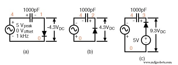
Consider a sinusoidal source of 5 V peak (V(4)) feeding a clamper as shown in Figure (a). During the first positive half‑cycle the diode conducts, charging the capacitor so that its left node rises to +5 V (≈+4.3 V after the diode drop). The right node then sits at –5 V relative to ground. When the source voltage again rises above the capacitor’s stored voltage, the diode conducts again, keeping the output’s positive peak from exceeding 0 V. The negative peak, however, swings to –5 V, so the waveform is effectively shifted upward by 5 V.
Variants:
- Figure (b): Diode reversed – negative peak is clamped to 0 V.
- Figure (c): Diode tied to a 5 V reference – negative peak is clamped to 5 V (≈4.3 V with diode drop).
SPICE model for the three configurations:
*SPICE 03443.eps
V1 6 0 5
D1 6 3 diode
C1 4 3 1000p
D2 0 2 diode
C2 4 2 1000p
C3 4 1 1000p
D3 1 0 diode
V2 4 0 SIN(0 5 1k)
.model diode d
.tran 0.01m 5m
.end
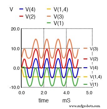
Explanation of nodes: V(4) is the 5 V peak source; V(1) is the output of Figure (a); V(1,4) is the DC voltage on the capacitor in Figure (a); V(2) is the output of Figure (b); V(3) is the output of Figure (c).
Changing the DC reference (e.g., from 5 V to 10 V) simply raises the clamped level; the waveform’s amplitude remains unchanged. Increasing the sine‑wave amplitude (from 5 V to 7 V) increases the output amplitude but the clamped peak stays at the reference.
Clamper Circuits as DC Restorers
In composite video systems (NTSC), sync pulses must remain at a fixed 100 % modulation level regardless of the picture’s brightness. A clamper, acting as a DC restorer, clamps the top of the sync pulses to a reference voltage that represents full modulation, preventing drift caused by varying video content.
Key points:
- A coupling capacitor alone produces a signal centered on its average DC level (usually 0 V).
- A clamper adds a DC reference and a diode, clamping one peak and shifting the waveform.
- Common applications include restoring sync levels in composite video.
Related worksheet: Clipper and Clamper Circuits Worksheet
Industrial Technology
- Foundations of DC Circuits: Understanding Direct Current and Core Electrical Concepts
- Understanding AC Circuits: A Beginner's Guide
- Rectifier Circuits: From Half‑Wave to Polyphase Full‑Wave Designs
- Peak Detector: How It Works and Practical Applications
- Understanding Clipper Circuits: Theory, Simulation, and Practical Applications
- Crystal and Transistor Radio Circuits: From Basic Detectors to Integrated AM/FM Receivers
- Analog vs. Digital Computational Circuits: A Practical Guide
- Control Circuits: Fundamentals, Applications, and Best Practices
- Bridge Circuits: Wheatstone, Kelvin, and Their Role in Precise Electrical Measurements
- Analyzing Complex RC Circuits Using Thevenin’s Theorem