


Amplifier Input and Output Impedance Analysis
Input impedance in transistor amplifiers varies markedly with circuit topology and biasing. While the true impedance is complex and frequency‑dependent, practical approximations give clear guidance for the three basic configurations.
For the common‑collector (emitter follower), the input resistance is simply the emitter resistance multiplied by the current gain:
Rin = \beta RE
In a common‑emitter stage the situation is slightly more involved because the internal emitter resistance, ree, must be considered:
Internal emitter resistance is given by:
ree = \dfrac{KT}{IE}\quad \text{where}\quad K = 1.38\times10^{-23}\,\text{W·s/K},\;T \approx 300\,\text{K}
For silicon transistors, the constant simplifies to approximately 26 mV per milliampere of emitter current:
ree \approx \dfrac{26\,\text{mV}}{IE\,(\text{A})}
Thus, the input resistance of a common‑emitter stage is:
Rin = \beta\,ree
Example: With \beta = 100 and an emitter bias of 1 mA,
ree = \dfrac{26\,\text{mV}}{1\,\text{mA}} = 0.26\,\Omega
Rin = 100 \times 0.26\,\Omega = 26\,\Omega
For a more accurate estimate in a common‑collector stage that includes an external emitter resistor RE, the input resistance becomes:
Rin = \beta\,(RE + ree)
This same expression also applies to a common‑emitter configuration that incorporates an emitter resistor.
The common‑base configuration has a markedly lower input impedance, essentially equal to the internal emitter resistance:
Rin = ree
High input impedance makes the common‑collector ideal for driving high‑impedance sources such as crystal or ceramic microphones. The low input impedance of the common‑base is useful in RF applications where a 50 Ω coaxial feed must be matched. The common‑emitter stage offers a moderate input impedance, making it suitable for mid‑range sources like dynamic microphones.
Output impedances for the three basic configurations are summarized in the figure below. The moderate output impedance of the common‑emitter stage explains its popularity for general amplification tasks. The very low output impedance of the common‑collector stage is exploited for impedance matching, for example, in transformer‑less connections to a 4 Ω speaker. Closed‑form expressions for output resistance exist but are more complex; see R. Victor Jones’ derivations (see reference [RVJ]).
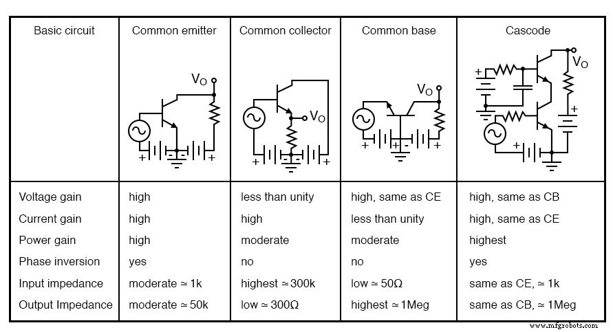
Amplifier characteristics adapted from the GE Transistor Manual, Figure 1.21.
Review
- Refer to the figure above for a visual comparison of input and output impedances.
Related Worksheets
- Class A BJT Amplifiers
Industrial Technology
- Common‑Emitter Amplifier: Design, Measurement, and Feedback Techniques
- Designing a High‑Gain Multi‑Stage Common‑Emitter Amplifier with Negative Feedback
- Designing a High‑Gain Differential Amplifier with NPN Transistors
- Non‑Inverting Amplifier: Build, Test, and Master Op‑Amp Gain Control
- Build a High‑Performance Class B Push‑Pull Audio Amplifier with TL082 Op‑Amp
- Understanding Amplifier Gain: Voltage, Current, and Power
- Common‑Collector Amplifier: Emitter‑Follower Fundamentals & Applications
- Common‑Base Transistor Amplifiers: Design, Analysis, and Applications
- Understanding Amplifier Feedback: Positive vs Negative, and Practical Applications
- Understanding Voltage Amplifiers: How They Boost Signal Voltage