Industrial manufacturing
Industrial Technology

Panelization is a must-have with the consideration of PCB manufacturing efficiency. On the one hand, panelization leads to the improvement of PCB manufacturing efficiency so that lead time can be reduced. On the other hand, for small PCBs with irregular shapes, panelization is the most effective

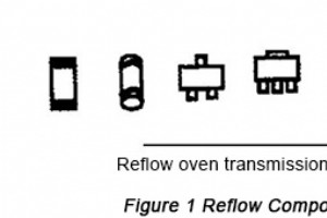
Development of modern scientific technology leads to the increasing miniature of electronic components and massive application of SMT technology and devices in electronic products. SMT manufacturing device has attributes of full auto, high precision and high speed. Because degree of automation ri
Modern electronic system is developing in the trend of small package, large scale and high speed as the density of chips is becoming increasingly large in SLSI (super-large-scale integration), which brings about some inevitable problems such as how to analyze and deal with the interconnections an
At present, the fast development of Internet technology witnesses the massive application of email, online payment and personal communication. Under this background, information security has been a critical research theme around the world. PKI (Public Key Infrastructure) technology provides secur

Development of communication technology has witnessed gradually wide applications of wireless radio frequency (RF) circuit such as in the fields of mobile phones, Bluetooth products and RF circuit has been the core technology of radio propagation. In recent years, however, the gradual prevalence
Nowadays, multilayer PCBs are used in most high-speed circuit systems and lots of circuit systems have numerous operating powers, providing strict requirements to image planes design, especially the settlement of relationships between multiple power/ground planes. Besides, special copper clad sur
As the commonest components integrated platform, multi-layer PCBs connect circuit boards and components together. With electronic products becoming light, thin and small in size, and having high performance, IC components have become highly integrated, leading to the high integrity of PCBs. As a
Fast development of electronic technology leads to instant improvement in terms of computational speed, computational frequency and integrity of electronic products. Besides, with the volume of electronic products shrinking, volumetric power density is becoming increasingly high. In addition, the
As an important carrier of all kinds of electronic components, printed circuit boards provide excellent mechanical support for components and connect those components through copper foil lines with different thickness and soldering pads with different sizes according to logical circuits to implem
Classification of Bottom Filling Technology Bottom filling can be classified into fluidity bottom filling based on capillary flow theory and nonfluidity bottom filling. Up to now, bottom filling technology suitable for chips of BGA, CSP etc. mainly includes: capillary bottom filling technolog
Printed circuit boards (PCBs) consist of anything from one layer to multiple layers of dielectric and conductive materials. When bonded into boards, these layers carry circuits that power a vast range of home electronics, such as alarm clocks, kitchen appliances, desk supplies, computers and
HDI, short for High Density Interconnection, is a type of printed circuit board technology starting to develop at the end of 20th century. For traditional PCB boards, mechanical drilling is utilized, with some disadvantages including high cost with aperture being 0.15mm and difficulty in improvem
Since its first use in highly reliable military equipment in 1980s, flex-rigid PCBs have been widely used in high-tech fields. Up to now flex-rigid boards have become one of the research hotspots in the PCB industry. Combining the supporting function contributed by rigid boards and the functions

In the sustainable development of IC (integrated circuit) design and manufacturing, the prominence of some problems such as signal transmission delay and noise plays a role in influencing integrity of signals. Therefore, sufficient attention must be paid to the problems in the process of PCB desi
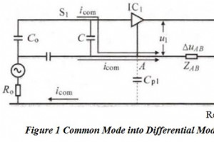
Ground in PCB • Influence of Common Code Interference to PCB Inner Signal Printed Circuit Board (PCB) inner printed lines feature parasitic parameters relative to reference ground board and when function signals are being transmitted inside PCB, the same equipotential node in the sa
Component layout has to meet the requirement of the whole machine electric properties & mechanical structure and the requirement of SMT production craft. Since its difficult to overcome product quality problem caused by design, PCB designers have to understand the basic SMT craft attributes a
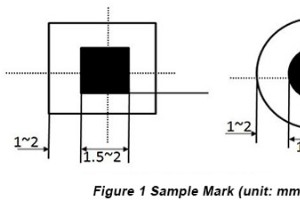
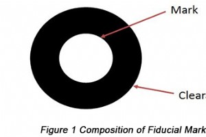
In order to correct the errors generated in the process of PCB fabrication, Mark refers to a set of patterns used for optical localization. Mark can be classified into PCB Mark and local Mark. Mark Patterns The shape and size of Mark should be designed according to the specific requiremen
The most basic form of design for manufacture as it applies to PCBs is the use design rules and design rule checking in PCB design software. Design rule checking (DRC) is the process of looking at a design to see if it conforms to the manufacturing capabilities of a PCB fabricator. Typically the
Compared with the development of software system, the hardware design and its optimization of electronics have seen the practical problems such as long time consumption and high cost. However, in the actual design, engineers tend to pay more attention to the highly principled issues but what lead
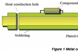
With power components coming in smaller and smaller surface mount packages it is important to come up with a coherent approach to mitigating the thermal dissipation demands of these components in a PCB design. While the development of an exact mathematical analysis of the thermal characteristics
Industrial Technology