Industrial manufacturing
Industrial Technology

Right now, high-speed PCB design has been widely applied in so many fields as telecommunication, computer and graph and image processing and all high-tech value added products are designed towards low power consumption, low electromagnetic radiation, high reliability, miniaturization and light we

The constant improvement of electronic product assembly density leads both electronics components and devices to miniaturization, fine pitch and even no leads. This article will discuss excellent solder paste printing technologies compatible with QFN (quad-flat no-leads) components and introduce
Along with the fast development of very large scale integrated circuits (ICs), electronics assembly demands can never be met by traditional package types and newer packages come into being due to the encouragement of demands in terms of higher integrity, smaller board size and higher I/O count. A
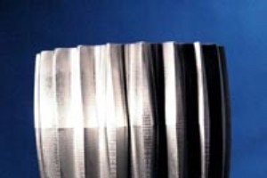
Vias play a role as conductors connecting traces across different layers of a multi-layer PCB (Printed Circuit Board). In the case of low frequency, vias don't affect signal transmission. As frequency rises (1GHz above) and signal rising edge becomes steep (1ns at most), however, vias can'
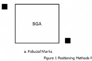
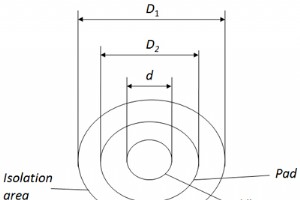
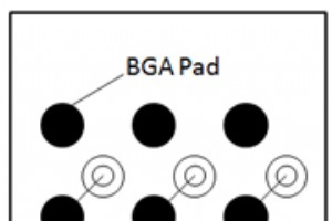
With the development of chip packaging technology, BGA (ball grid array) has been regarded as a standard packaging form. As far as chips with hundreds of pins are concerned, the application of BGA package brings forward tremendous advantages. BGA chips win over QFP (quad flat package) chips in
LED (Light Emitting Diode) display has been embraced by electronic industries owing to its merits ranging from high lightness, low energy consumption, long lifetime to stability. Due to the constant progress on technical indexes like pitch, stability, lightness or color depth (grayscale), printed
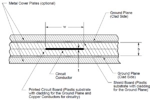
Nowadays have witnessed wide applications of RF/Microwave PCBs in numerous handheld wireless devices and commercial industries including medical, communication, etc. Since RF (radio frequency)/Microwave circuits are distributed parameter circuits that tend to generate skin effect and coupling eff
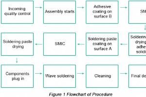
Quality of electronic products largely depends on assembly technologies. Box build assembly refers to a process during which according to design files, work procedure and technologies, multiple components and accessories are assembled and fixed on certain positions of circuit boards or enclosures
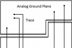
EMC, short for Electro-Magnetic Compatibility, refers to a coexistence state in which electronic devices are capable of implementing their own functions in the same electromagnetic environment. Put it simply, EMC allows electronic devices to work independently and normally with no interference be
When it comes to laptop PCBs, 6-layer or 8-layer circuit board is generally selected. Based on cost consideration, however, 6-layer PCB is an optimal selection for PCB designers. Sadly, EMC (Electromagnetic Compatibility) design for 6-layer PCB has been plaguing board designers. Laptop develop
PCB Requirement for Mil/Aero Electronic Products When electronic engineers are preparing for PCB design for military/aerospace (short form as "mil/aero") applications, some details and performance requirement have to be taken into consideration. It's generally known that both mi

Thin-film micro-strip circuits have been widely applied in microwave communications, electronic countermeasure (ECM), aerospace industry etc. When manufacturing thin-film ICs (Integrated Circuits), it is very important to apply deposited thin-film resistor material to fabricate high-accuracy and
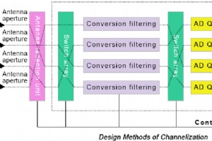
With the development of micro-electronics and bandwidth device technology pushing digitalization forward, RF integration will climb to a higher level with wider bandwidth and gradual reduction in terms of volume, weight and cost. Moreover, revolutionized changes will take place on system hardware
Electrical products are born with EMI (Electro-Magnetic Interference). Multifunction of electronic products meet people's different expectations, which also leads to the generation of a series of EMI issues that directly threaten people's health and environmental security. Effect of EMI o
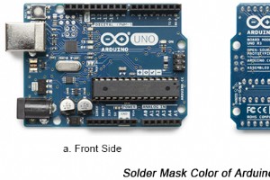
What is Solder Mask? Solder mask, also called solder resist or solder-stop mask/coating, is a thin layer covering copper traces without necessity of soldering on a printed circuit board (PCB) on both top side and bottom side to help ensuring PCB reliability and high performance. Resin is usu
With the flourishing and wide application of laptops, it has become overarching to improve product quality and manufacturing efficiency and key technique and product quality control in the process of laptop production have attracted the most concentration. Based on the analysis on key technique i
With constant progress of electronic technologies, increasing high frequency of clock in digital system, increasingly short rising edge time, PCB system has become a system structure with high performance, far more than just a platform supporting components. From the perspective of electric perfo
As a platform for components whose applications can be well implemented in electronic products, PCBs (Printed Circuit Boards) play a key role as electric connection between components and account for the base in electronic devices or equipment. Therefore, its performance and quality directly lead
In the process of electronic system whose clock frequency increasingly rises, signal integrity issues come out gradually such as incorrect timing sequence and incorrect reflection of transmission lines, badly influencing the normal running of circuit system. Furthermore, traces on PCB become so c
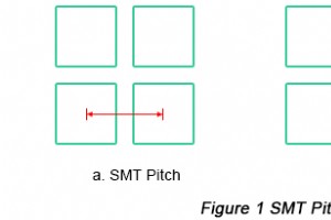
With the development of electronic component package technologies towards miniature, light weight and high performance, it has been a development trend of electronic components to increase component function density and decrease spacing between input terminals and output terminals, which is best
Industrial Technology