


Power‑up Phase Determinism: Leveraging Multichip Synchronization in High‑Speed ADC/DAC Platforms
The integration of multiple digital signal processing blocks, wideband DACs and ADCs into a single monolithic chip now enables the off‑load of power‑hungry FPGA resources. This results in smaller, lower‑power platforms that support higher channel counts and sampling rates than ever before. Crucially, these advanced ICs incorporate multichip synchronization (MCS) algorithms that provide a deterministic phase across all channels at power‑up, eliminating the need for complex system‑level calibration to align front‑end networks.
High‑Level System Block Diagram
The test system illustrated in Figure 1 comprises four integrated DAC/ADC/DSP ICs, each containing four 12 GSPS DACs, four 4 GSPS ADCs, and 12 digital up‑converters (DUCs) and 12 digital down‑converters (DDCs). The entire array is driven by a single 500 MHz reference clock, which is distributed to four PLL synthesizers that generate the 12 GHz clock required by each digitizer IC. An RF front end is attached to every input and output, providing filtering and amplification for the edge‑launched RF connectors. All signals are powered from a single 12 V supply, with transmit paths routed on the board’s bottom layer and receive paths on the top to maximise channel‑to‑channel isolation.
click for full size image
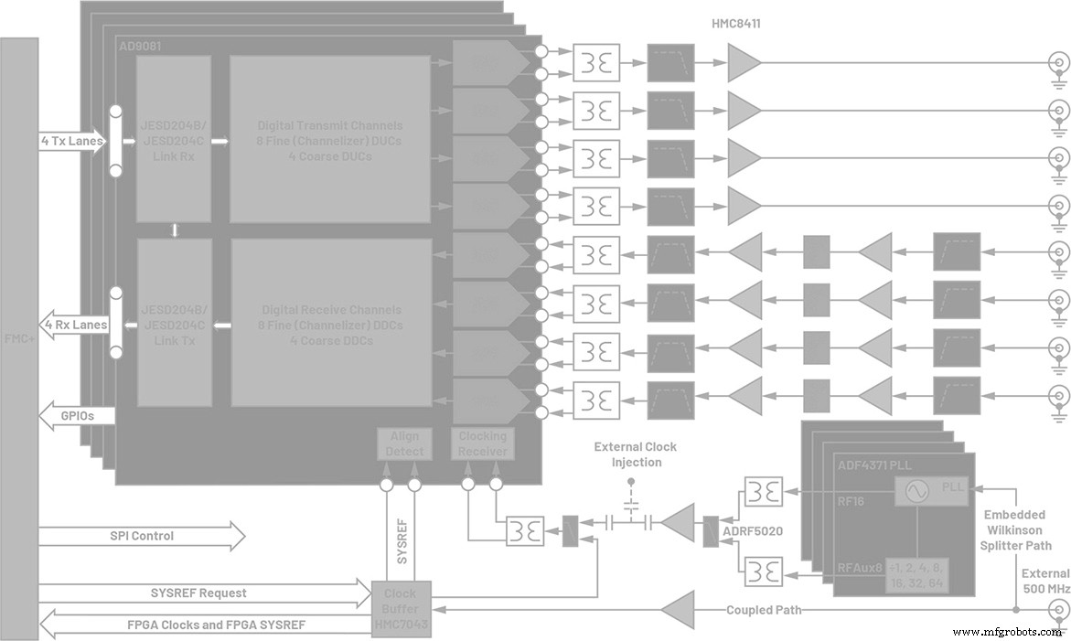
Figure 1. High‑level block diagram of the system used to demonstrate MCS and multichannel calibration algorithms. (Source: Analog Devices)
Subarray Clock Tree Structure
The clock tree is built around a single 500 MHz reference that feeds four PLL synthesizers and a reference‑locked buffer that generates the system reference signals (SYSREFs) and baseband processor (BBP) clocks. This architecture offers three key benefits:
- Individual channel SYSREF delays correct trace‑length mismatches between ICs.
- Per‑PLL phase adjustment synchronises all digitizer clocks and compensates for thermal gradients.
- User‑defined SYSREF delays satisfy the setup‑and‑hold requirements of each digitizer.
The buffer IC’s analog fine‑delay taps enable the SYSREF pulse to reach all ICs within the same sample‑clock cycle, providing a single‑phase reference that can be corrected in software or hardware.
Digital Interface with Baseband Processor
Each digitizer establishes a JESD204B or JESD204C link with the BBP. The link parameters—number of lanes (L), converter resolution (N’), and virtual converters (M)—determine the data bandwidth. In this study, the DAC links use M = 16, N’ = 16, L = 4, while the ADC links use M = 8, N’ = 16, L = 2. With a 250 MSPS I/Q data rate, the lane rate is 16.5 Gbps for both ADC and DAC sides, calculated as follows:

and for JESD204B:

The links operate in JESD204C Subclass 1, which uses SYSREF to align the local extended multiblock counter (LEMC). The LEMC runs at 7.8125 MSPS (F = 8 octets per frame, K = 32 frames per multiframe). Deterministic phase across arbitrary RF frequencies requires the LEMC rate to remain constant even as the system temperature changes.
Multichip Synchronization Method
The integrated ADC/DAC ICs provide MCS circuitry that guarantees deterministic phase on all transmit and receive RF channels, even when the DUC/ DDC DSP blocks are active. During factory calibration, a lookup table (LUT) is populated so that each power‑up achieves the same phase alignment, regardless of RF frequency, thermal drift, or system reset.
Figure 2 illustrates the two‑step MCS workflow:
click for full size image
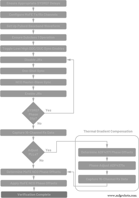
Figure 2. MCS workflow aligns both data lanes and internal NCOs across the entire subarray. (Source: Analog Devices)
The algorithm is split into:
- One‑shot sync – aligns the JESD data lanes of all digitizers by synchronising the SYSREF and LEMC boundaries.
- NCO master‑slave sync – aligns all internal NCOs by routing a GPIO‑based trigger through the BBP.
During one‑shot sync, the user defines the JESD parameters and configures optional SYSREF averaging. The system then issues a simultaneous SYSREF pulse to all ICs. The resulting SYSREF‑LEMC phase register is polled; a zero value confirms alignment. Next, the master‑slave sync assigns one IC as the master; its GPIO0 output drives the GPIO0 inputs of the remaining ICs. Triggering on the LEMC rising edge resets the NCOs of every slave, locking them to the master’s phase.
click for full size image
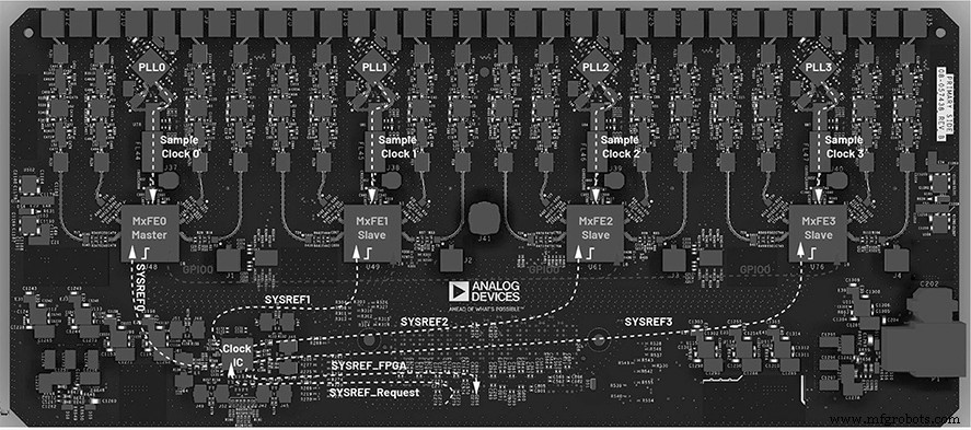
Figure 3. SYSREF signals enable one‑shot sync; GPIO signals enable NCO master‑slave sync, achieving deterministic phase. (Source: Analog Devices)
After both steps, the receive DDCs and transmit DUCs exhibit repeatable phase offsets across 100 power cycles, even under a static thermal gradient. Figure 4 shows the calibrated phase offsets tightly clustered for each channel, confirming deterministic behavior for all eight DDCs and eight DUCs.
click for full size image
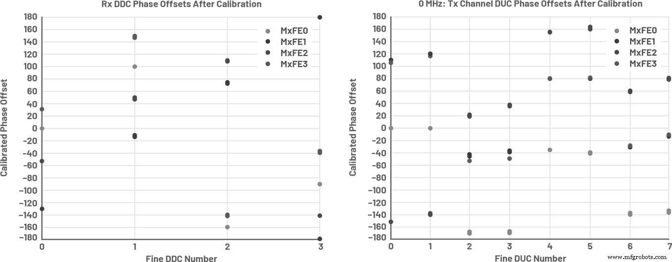
Figure 4. Receive fine DDCs (left) and transmit fine DUCs (right) remain aligned after repeated power‑cycles. (Source: Analog Devices)
When the MCS algorithm is executed at boot‑up, deterministic phase is established as long as the PLL synthesizers maintain their phase relationship with the SYSREF signals. To counteract thermal‑drift‑induced PLL phase changes, the platform incorporates PLL synthesizer phase adjustments that preserve the alignment.
In the next installment, we will explore PLL phase adjustments in detail, examine scalability to multiple subarrays, and present system‑level calibration algorithms that build on this deterministic foundation.
References
1. Del Jones, “JESD204C Primer: What’s New and in It for You—Part 1.” Analog Dialogue, vol. 53, no. 2, June 2019.
2. Del Jones, “JESD204C Primer: What’s New and in It for You—Part 2.” Analog Dialogue, vol. 53, no. 3, July 2019.
Embedded
- Understanding AC Phase Shift: How Waveforms Lead and Lag
- Cuckoo Clock: History, Craftsmanship, and Modern Evolution
- Mastering C# Using Statements: Imports, Aliases, and Static Directives
- Ensuring Power‑Up Phase Determinism with PLL Synthesizers and System‑Level Calibration
- Mastering Asynchronous Reset Synchronization in ASICs and FPGAs
- High‑Precision Waveform Generation with a DAC‑Based Custom PCB
- Build a Stylish Wall Clock with Adafruit 60‑LED Neopixel Ring & Arduino
- Build Your Own 3D Printed Lunar Phase Clock – Step-by-Step Arduino Guide
- Build a Precise Clock with Arduino Nano and 16x2 LCD
- Leveraging Phase Diagrams to Accurately Predict Vapor Pressure Curves