


Using the 4511 7‑Segment Decoder: A Practical BCD Display Tutorial
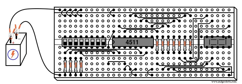
Parts & Materials
- 4511 BCD‑to‑7seg latch/decoder/driver (Radio Shack catalog # 900‑4437)
- Common‑cathode 7‑segment LED display (Radio Shack catalog # 276‑075)
- Eight‑position DIP switch (Radio Shack catalog # 275‑1301)
- Four 10 kΩ resistors
- Seven 470 Ω resistors
- One 6 V battery
⚠️ Caution: The 4511 IC is CMOS and highly sensitive to static discharge. Handle with care and use an antistatic wrist strap.
Cross‑References
Lessons In Electric Circuits, Volume 4, Chapter 9: “Combinational Logic Functions.”
Learning Objectives
- Understand how to use the 4511 7‑segment decoder/display driver IC.
- Familiarize with Binary‑Coded Decimal (BCD) representation.
- Create decimal digit displays using 7‑segment LED assemblies.
- Identify and work with both active‑low and active‑high logic inputs.
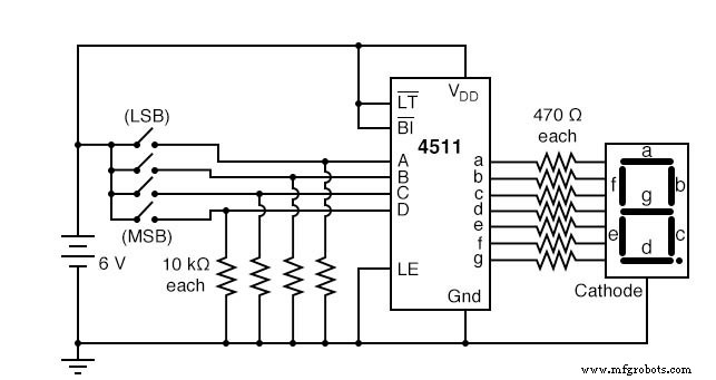
Schematic Diagram
Illustration
Instructions
This exercise introduces the 4511 decoder/display driver IC, a common component in digital devices. The IC accepts a four‑bit BCD input and energizes the appropriate output lines (a‑g) to display the corresponding decimal digit on a 7‑segment LED.
The BCD inputs are labeled A, B, C, and D (least‑significant to most‑significant). Each output connects to a 470 Ω series resistor before reaching the LED segment. The 4511 requires a common‑cathode display, which is used here.
After assembling the circuit and applying power, use the DIP switches to step through binary values 0000 to 1111. Observe the display: 0000 should show "0", 0001 should show "1", and so on up to 1001 (decimal "9"). Values 1010‑1111 represent binary numbers beyond a single decimal digit and are undefined in BCD. The datasheet explains that the IC will either blank the display or show an undefined pattern for these inputs.
Three pins on the 4511 are permanently tied to VDD or ground: Latch Enable (LE), Blanking Input (BI), and Lamp Test (LT). To explore their functions, disconnect each pin one at a time and replace the short jumper with a longer wire that can be switched to the opposite rail.
For example, remove the jumper on pin 5 (LE) that connects to ground, then use a long jumper to toggle it to VDD. Vary the BCD inputs and observe how the display changes. Once you understand LE’s role, reconnect it to its default rail and experiment with BI and LT.
BI and LT are active‑low inputs (indicated by a bar over the abbreviation), meaning they perform their function when pulled low. LE is active‑high, so it activates when pulled high. Refer to the 4511 datasheet for detailed behavior and recommended operating conditions.
Safety & Troubleshooting
- Always double‑check resistor values to avoid exceeding the LED current rating.
- Verify correct pin‑to‑pin connections on the 4511: A‑D (1‑4), LE (5), a‑g (6‑12), BI (13), LT (14), VDD (15), VSS (8).
- If the display does not respond, confirm that the common‑cathode connections are correct and that no pins are floating.
- Use a multimeter to test continuity and ensure the battery is supplying 6 V.
Industrial Technology
- Non‑Inverting Amplifier: Build, Test, and Master Op‑Amp Gain Control
- Understanding Multiple-Input Logic Gates: Functions, Truth Tables, and Practical Applications
- Mastering the D Latch: A Clean 1‑Bit Memory Circuit
- Understanding the J‑K Flip‑Flop: Design, Logic, and Applications
- Monostable Multivibrators (One‑Shots): Design, Timing, and Industrial Applications
- Display Tubes: From CRTs to Cat‑Eye Indicators
- Advanced Spectrum Analysis: Interpreting Waveforms and Harmonics
- Mastering Method Overloading in C#: Concepts, Examples, and Best Practices
- Understanding Verilog Tasks: Functions vs Tasks, Syntax, and Usage
- Mastering D Latches: Design, Operation, and Key Differences