


Full Adder: Building Efficient Multi‑Bit Binary Adders
When you add more than two binary digits, a single half‑adder is no longer sufficient. The traditional approach—creating a truth table for each new width—is accurate but slow. A full adder overcomes this by handling a third input, the carry‑in, allowing the design to scale quickly and reliably.
Consider a two‑bit addition:
    11
+   11
-------
    110
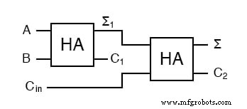
The middle column requires three inputs: a, b, and the carry‑in Cin. Using a two‑input adder as a building block, we can construct a three‑input adder that produces both a sum bit and a carry‑out.
Mathematically, if Σ = a + b + Cin and Σ1 = a + b, then Σ = Σ1 + Cin. The images below illustrate the logic diagram for this configuration.
Let’s examine the truth table for a three‑input sum:
Cin + a + b = ?
0 + 0 + 0 = 0
0 + 0 + 1 = 1
0 + 1 + 0 = 1
0 + 1 + 1 = 10
1 + 0 + 0 = 1
1 + 0 + 1 = 10
1 + 1 + 0 = 10
1 + 1 + 1 = 11
The low‑order bit is correctly produced by the XOR of the three inputs. The high‑order carry appears when either
a + b generates a carry (C1) or when a + b produces a sum bit and the carry‑in is one. Hence the carry‑out logic is Cout = C1 OR (Σ1 AND Cin).
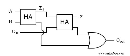
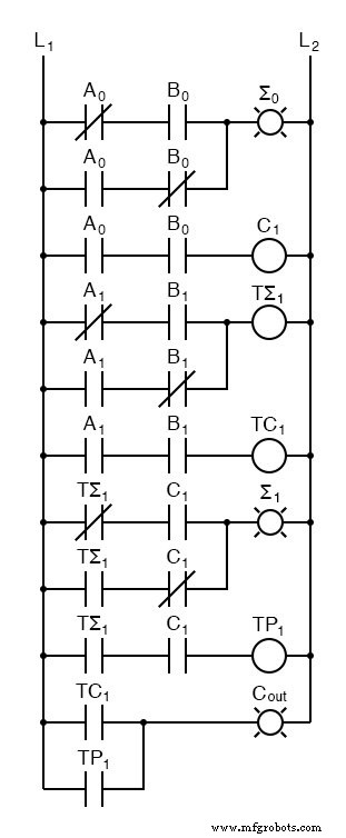
In some applications, replacing the final OR gate with an XOR gate eliminates a gate without altering functionality, reducing propagation delay.
By cascading two full adders, we can add two‑bit numbers efficiently. The diagram below shows the wiring of two full adders for a 2‑bit adder:
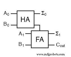
Here, A0 and A1 are the low‑ and high‑order bits of operand A; similarly for B. The outputs Σ0 and Σ1 form the 2‑bit sum, and Cout propagates to the next stage.
While a 2‑bit adder can be built directly from logic gates, using full adders for both bit positions streamlines larger designs and facilitates chaining. This approach scales naturally: a 4‑bit adder is two 2‑bit adders linked by carry; an 8‑bit adder is two 4‑bit adders, and so forth.
Below is an example of an 8‑bit adder constructed from full adders:
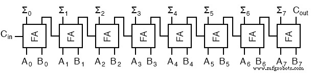
Each "2+" block represents a 2‑bit adder, each "4+" block a 4‑bit adder, and the combined 8‑bit adder achieves the same result as a monolithic 8‑bit design. The trade‑off is that a hierarchical design incurs additional propagation delay through the carry chain, whereas a single‑stage sum‑of‑products implementation may offer faster timing at the cost of design complexity.
For large combinational circuits, designers typically choose between modular construction—simpler to design but potentially slower—and monolithic design—faster propagation but more complex synthesis. The full‑adder approach exemplifies modularity, allowing incremental verification and reuse.
Related Worksheet:
- Binary Math Circuits Worksheet
Industrial Technology
- Electronics: A Hands‑On Science for All
- Setting Up a Home Electronics Lab: Tools, Work Area, and Supplies
- Mastering Voltmeter Use: Accurate Voltage Measurement Made Simple
- Mastering Ohmmeter Measurements: A Practical Guide to Resistance Testing
- Building and Troubleshooting a Basic 6‑V Battery‑Lamp Circuit
- Measuring Current with an Ammeter: A Practical Guide
- Full Adder: Building Efficient Multi‑Bit Binary Adders
- Designing a Binary Half‑Adder: From Logic Gates to Ladder Diagrams
- Verilog Full Adder Design & Implementation Guide
- Ripple Carry Adder Explained: Key Concepts & Applications