Industrial manufacturing
Nanomaterials

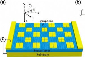
AbstractA graphene-loaded metamaterial absorber is investigated in the mid-infrared region. The light-graphene interaction is greatly enhanced by virtue of the coupled resonance through a cross-shaped slot. The absorption peaks show a significant blueshift with increasing Fermi level, enabling a wid
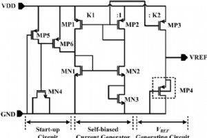
AbstractIn this paper, a nano-watt resistorless subthreshold voltage reference with high-power supply rejection ratio (PSRR) is presented. A self-biased MOS voltage divider is proposed to provide bias current for whole voltage reference, which is a positive temperature coefficient (TC) current conta
AbstractWe present an all‑dielectric gradient metasurface composed of a periodic array of cross‑shaped silicon nanoblocks on a fused‑silica substrate that functions as a polarization beam splitter in the visible spectrum. By engineering two opposing transmission‑phase gradients along the x‑direction
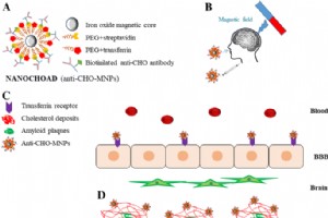
Abstract Alzheimer’s disease (AD) remains one of the most costly neurodegenerative disorders worldwide, underscoring the urgency for non‑invasive, early‑diagnostic tools. Emerging evidence links abnormal cholesterol accumulation around senile plaques to AD pathogenesis, suggesting cholesterol as a v
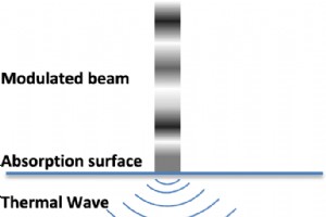
AbstractModulated continuous‑wave (CW) lasers trigger a photothermal response that rapidly absorbs light and generates thermal waves around irradiated nanostructures. In this study, we explore how such laser irradiation influences particle fragmentation and consequently improves the thermal diffusi
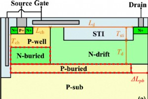
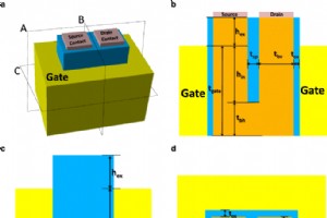
Abstract We present a lateral double‑diffused MOS (LDMOS) transistor that achieves an unprecedented specific on‑resistance (Ron,sp) of 8.5 mΩ·mm² while delivering a 43 V breakdown voltage (BV). The device incorporates an enhanced dual‑gate architecture, formed by a highly doped N‑buried layer beneat
AbstractThis study introduces a silicon‑based photodetector that couples a sub‑wavelength gold grating with a resonant cavity to realize near‑infrared (NIR) polarimetric detection. The gold–silicon Schottky interface harvests hot electrons generated by surface plasmon resonances, extending silicon’s
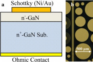
Abstract Vertical GaN Schottky barrier diodes (SBDs) grown on Ge‑doped free‑standing GaN substrates exhibit superior crystal quality and electrical performance. Cathodoluminescence imaging reveals a uniform dislocation density of ≈1.3×106 cm−2. The devices present a low turn‑on voltage Von of 0.70–0
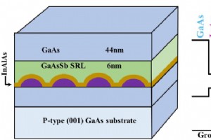
Abstract In this study we investigate how thin In0.15Al0.85As interlayers influence the optical behavior of InAs quantum dots (QDs) capped with a GaAs0.85Sb0.15 strain‑reducing layer (SRL). Using high‑resolution X‑ray diffraction (HRXRD) and 77 K photoluminescence (PL) spectroscopy, we compare sampl
AbstractA novel high-performance rectangular gate U channel FET (RGUC FET) for extreme integrated distance between source and drain contacts is proposed in this paper. The RGUC FET represents nearly ideal subthreshold characteristics till the distance between source/drain (S/D) contacts reduced to 2
AbstractThe geometric phase is an extra phase evolution in the wave function of vibrations that is potentially applicable in a broad range of science and technology. The characteristics of the geometric phase in the squeezed state for a carbon-nanotube-based nanowire resonator have been investigated
AbstractWe demonstrate the catalyst‑free, plasma‑assisted molecular beam epitaxy (PA‑MBE) growth of single‑crystalline gallium nitride (GaN) nanowires directly on indium tin oxide (ITO)–coated fused silica. By carefully tuning growth temperature and beam equivalent pressure (BEP), we achieve vertica
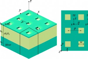
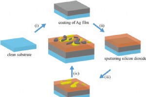
AbstractWe introduce a broadband, high‑efficiency absorber that harnesses the void plasmon (VP) effect within a Fabry–Perot (FP)‑like architecture. The structure consists of a perforated silver film, an aluminum‑oxide spacer, and a continuous silver ground plane. The hybrid FP/VP resonance delivers
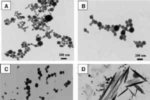
AbstractHemin, a highly bioavailable iron source, is limited by its negligible aqueous solubility. We report a simple dialysis‑based approach that yields two distinct hemin nanoparticle morphologies—tadpole‑shaped (≈200 nm head, 100 nm tail) and sphere‑shaped (50–100 nm). Both forms exhibit dramatic
Abstract90 % efficiency across the visible and near‑infrared spectrum. This approach offers a scalable, tunable platform for high‑performance absorbers.IntroductionSub‑wavelength absorbers, often referred to as metal‑insulator‑metal (MIM) structures, have attracted significant attention due to their
AbstractAccurate, rapid monitoring of Fe³⁺ is essential for health and environmental safety. We report, for the first time, TiO₂ nanotube arrays decorated with Ag nanoparticles that achieve a sensitivity of ~30 µA µg⁻¹ L and a detection limit of 15 nM for Fe³⁺ using anodic stripping voltammetry. The
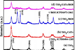
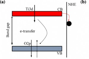
Abstract Hollow, heterostructured nanocomposites are a proven strategy for boosting photocatalytic activity. We engineered a ternary TiO2/CdTe/BiOI system in which TiO2 hollow microspheres serve as the scaffold, CdTe quantum dots (QDs) act as electron donors, and BiOI flakes provide visible‑light ha
AbstractWith Moore’s law closing to its physical limit, traditional von Neumann architecture is facing a challenge. It is expected that the computing in-memory architecture-based resistive random access memory (RRAM) could be a potential candidate to overcome the von Neumann bottleneck problem of tr
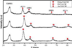
AbstractThe aim of this study was to synthesize, characterize, and observe the catalytic activity of Pd1Au1 supported by vapor-grown carbon nanofiber (VGCNF) anode catalyst prepared via the chemical reduction method. The formation of the single-phase compounds was confirmed by X-ray diffraction (XRD
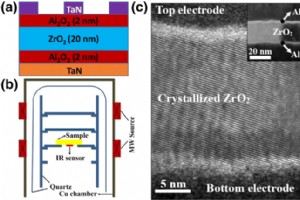
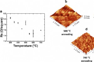
AbstractMetal‑insulator‑metal (MIM) capacitors are pivotal in RF, DRAM, and mixed‑signal ICs, where ever‑increasing capacitance density is required as device dimensions shrink. In this study, microwave annealing (MWA) is employed to enhance the dielectric properties of Al₂O₃/ZrO₂/Al₂O₃ (A/Z/A) MIM c
Nanomaterials