

Industrial manufacturing
Nanomaterials

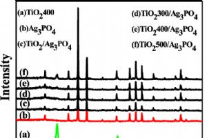
Abstract We present a simple, scalable two‑step route to Ag3PO4/TiO2 heterostructures that deliver outstanding visible‑light photocatalytic performance. The composites were comprehensively characterized by X‑ray diffraction (XRD), scanning electron microscopy (SEM), transmission electron microscopy
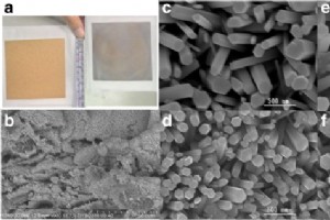
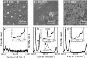
Abstract We present a flexible photocatalytic paper that combines Cu2O and Ag nanoparticles (NPs) with ZnO nanorods (NRs) to achieve efficient visible‑light degradation of organic dyes. ZnO NRs are hydrothermally grown on kraft paper, then selectively decorated with Cu2O, Ag, or both NPs via photore
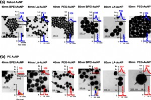
AbstractGold nanoparticle (AuNP)–protein corona complexes can alter cytochrome P450 (CYP)-mediated testosterone (TST) metabolism by changing their physicochemical properties. We examined how NP size, surface chemistry, and human plasma protein corona (PC) influence TST metabolism in pooled human liv
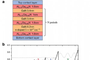
Abstract We investigated how interface roughness, non‑intentional doping, and alloy disorder affect the optical gain of GaN‑based terahertz quantum cascade lasers (QCLs) using the nonequilibrium Green’s‑function (NEGF) formalism. Our simulations show that alloy disorder has a negligible impact on ga
AbstractAchieving high‑quality graphene on insulating substrates is pivotal for next‑generation graphene electronics. Here we report a catalyst‑free, atmospheric‑pressure chemical vapor deposition (APCVD) method that directly grows mono‑ to few‑layer graphene on SiO₂ using ethanol as a liquid hydroc
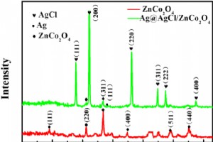
AbstractIn this work, a comprehensive investigation of the composite Ag@AgCl/ZnCo2O4 microspheres photocatalyst, prepared by a facile two-step method, is presented, and using complementary characterization tools such as X-ray diffraction (XRD), scanning electron microscopy (SEM), energy dispersive X
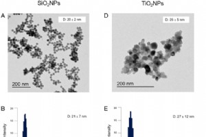
Abstract The increasing incorporation of nanoparticles (NPs) into consumer products has outpaced comprehensive safety evaluations. This study investigates how the physicochemical attributes of SiO₂ and TiO₂ NPs influence cellular uptake, intracellular trafficking, and mechanical perturbations in two
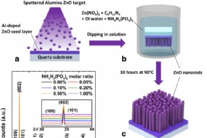
AbstractWe report the successful hydrothermal synthesis of phosphorus‑doped ZnO nanorods and systematically investigate how the dopant concentration alters their crystal structure, morphology, electrical behavior, and photoluminescence (PL) across the ultraviolet (UV), visible, and near‑infrared (NI
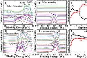
Abstract Bi‑layer architectures are routinely employed to enhance the reliability of conductive‑bridge random‑access memory (CBRAM). Here we introduce a cost‑effective, CMOS‑compatible method that generates a Ta2O5/TaOx bi‑layer through a low‑temperature anneal. The TaOx overlayer serves as an exte
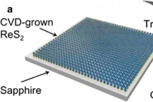
Abstract We report the first fabrication of a ReS₂/GaAs heterostructure via chemical vapor deposition and its deployment as a saturable absorber (SA) in a passively Q‑switched Nd:YVO₄ laser. The device achieves a record‑shortest pulse width of 51.3 ns at a repetition rate of 452 kHz, delivering 465
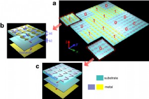
AbstractWe present a novel coding electromagnetic metasurface (EMMS) that unifies broadband, tunable radiation with low‑scattering behavior. Anisotropic unit cells exhibiting opposite phase responses to x- and y-polarized incidence are defined as binary elements “0” and “1”. Using a simulated‑anneal
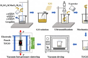
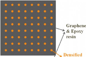
Abstract Ti matrix composites containing 1–5 wt % graphene oxide (GO) were fabricated by hot‑press sintering under argon. The reaction between Ti and GO produced TiC nanoparticles in situ, while a lamellar GO network was partially retained. Increasing GO loading and sintering temperature raised the
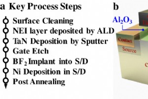
AbstractWe introduce a novel ferroelectric field‑effect transistor (FeFET) that incorporates nanocrystal‑embedded‑insulator (NEI) technology, enabling a remarkably thin unified ferroelectric/dielectric (FE/DE) gate stack. This architecture delivers low‑voltage logic operation and a non‑volatile memo
AbstractAll‑inorganic CsPbI₂Br perovskite solar cells (PSCs) exhibit superior thermal stability compared to hybrid counterparts, yet their power conversion efficiencies (PCEs) remain below the state‑of‑the‑art hybrid devices. In this study, we introduce a dual‑dopant strategy—co‑incorporating ZnCl₂
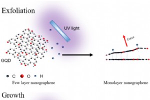
AbstractGraphene has been widely used in novel optoelectronic devices in decades. Nowadays, fabrication of large size monolayer graphene with spectral selectivity is highly demanded. Here, we report a simple method for synthesizing large size monolayer graphene with chemical functionalized groups in
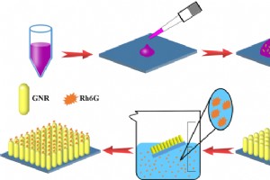
AbstractThe unique photonic behavior of self‑assembled metal nanoparticles underpins a broad range of optical technologies. Here, we report a facile evaporation‑based method to fabricate vertical arrays of gold nanorods (GNRs) on silicon wafers. By modulating the immersion time of the arrays in prob
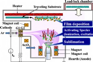
AbstractVertically aligned carbon nanotube arrays (VACNTs) are key to next‑generation thermal interface materials (TIMs). While thermally oxidized SiO2 has traditionally served as a buffer layer, atomic layer deposition (ALD) offers a route to fabricate pinhole‑free, dense oxides such as Al2O3, TiO
Abstract 10 nm, versus 6.6–6.8 g cm⁻³ for t < 10 nm. We provide quantitative insight into the size effect for films thinner than 10 nm, showing that the ratio of t to the electron mean free path (λ) controls µH. Introduction 100 cm² V⁻¹ s⁻¹ in hydrogenated or Ce‑doped In₂O₃ polycrystalline films, e
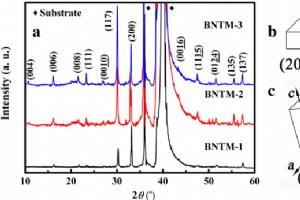
Abstract Bi₃.₁₅Nd₀.₈₅Ti₂.₉₉Mn₀.₀₁O₁₂ (BNTM) thin films were fabricated in three distinct crystallographic orientations—(200), (117) and mixed—using a sol‑gel route. Polarization fatigue was examined from 200 K to 475 K, revealing contrasting temperature dependencies: (200)-oriented films exhibited
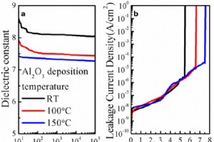
AbstractWe demonstrate that a‑IGZO thin‑film transistors (TFTs) fabricated with an O₂ plasma‑enhanced ALD Al₂O₃ gate dielectric deposited at room temperature (RT) exhibit outstanding performance: a field‑effect mobility of 19.5 cm² V⁻¹ s⁻¹, a subthreshold swing (SS) of 160 mV dec⁻¹, a threshold volt
Nanomaterials
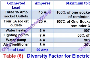
Understanding the Diversity Factor in Electrical Wiring: Why It Matters for Cable Sizing

CNC Machining vs. 3D Printing: Choosing the Right Manufacturing Method for Your Project
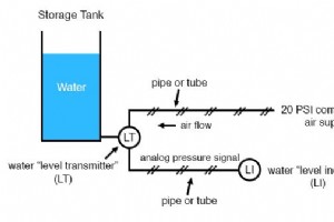
Analog and Digital Signals: Foundations of Industrial Instrumentation

Mastering Voltmeter Use: Accurate Voltage Measurement Made Simple
