


Expert Interview: Simon Fried, Co‑Founder of Nano Dimension, on 3D Printing’s Future in Electronics

The electronics industry is rapidly embracing additive manufacturing, reshaping how we develop everything from drones and satellites to laptops and smartphones. Yet at its core, any electronic system depends on components—printed circuit boards (PCBs), antennas, sensors—that have traditionally been costly and time‑consuming to produce. 3D printing is redefining this landscape by delivering faster product cycles, greater design freedom, and the ability to create non‑planar geometries that were previously unattainable.
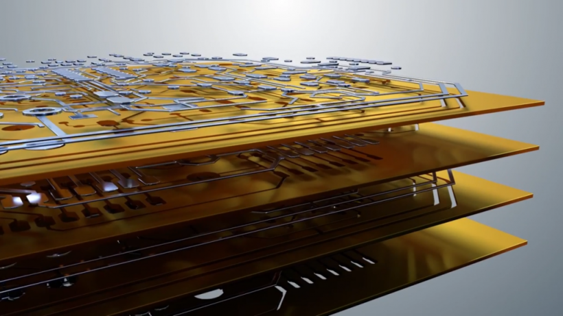
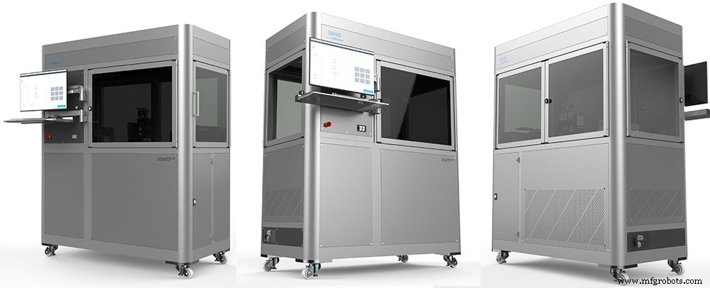
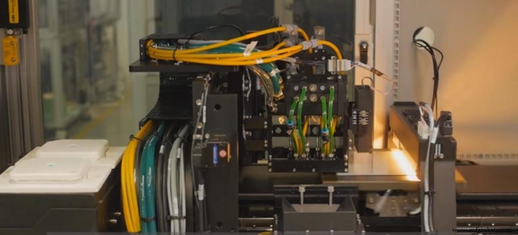
Founded in 2012 in Israel, Nano Dimension has become a global leader in additive manufacturing for printed electronics. Their proprietary DragonFly Pro system can simultaneously print metals and dielectric polymers, enabling companies to prototype electronics in-house, reduce lead times, and lower costs.
In this week’s Expert Interview, we spoke with Simon Fried, Co‑Founder and President of Nano Dimension, about the growing impact of 3D printing in electronics and how the company is pioneering this emerging field.
Can you tell us a bit about Nano Dimension?
Nano Dimension focuses exclusively on additive manufacturing for electronics. Traditionally, electrical engineers were forced to outsource circuit design and prototyping, which added significant lead time and cost. By bringing 3D printing into the electrical domain, we give engineers the freedom, flexibility, and confidentiality they need to test and iterate ideas in a practical, mechanical context.
Speaking specifically about your DragonFly Pro System technology, could you touch more on the value it brings to the table?
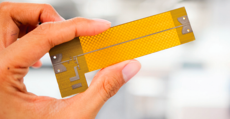
Imagine an electrical engineer tasked with designing the next PCB for a product. The process typically involves complex EDA (Electronic Design Automation) software, extensive simulation, and then sending the design to a third‑party manufacturer—an operation that can take weeks. With Nano Dimension’s system, engineers can design and fabricate a physical board in roughly 24 hours, instantly validating layouts, spotting errors, and exploring design improvements.
Our customers have reported transforming a six‑week engineering effort into a day and a half by printing prototypes themselves, eliminating the need to wait for external suppliers.
By eliminating the middleman for prototyping, we empower companies to test more ideas, iterate rapidly, and maintain secrecy. When development is fast and inexpensive, the cost of failure drops, encouraging greater innovation.
Defense firms, in particular, are drawn to our technology because they face strict constraints on design disclosure and supplier selection. Our system allows them to prototype critical components internally, ensuring compliance and confidentiality.
What other benefits does additive manufacturing offer electronics?
Additive manufacturing enables shapes and geometries that are impossible with conventional planar manufacturing—an exciting frontier for electrical engineers accustomed to flat, two‑dimensional layouts.
Traditional electronics fabrication is highly constrained, dictated by the manufacturing process and available components. Additive manufacturing lifts these constraints, opening a vast array of new design possibilities. Engineers can now create truly three‑dimensional PCBs, antennas, and other functional parts, moving beyond the limitations of flat traces.
Our vision is two‑fold: first, to make conventional PCB and RF electronics faster, cheaper, and more independent; second, to enable entirely new products that blend structural and electrical functions in unprecedented ways.
What are some of the challenges involved in 3D printing electronics?
Printing metals and polymers simultaneously is inherently complex. Metals require elevated temperatures and precise control, while polymers have different optimal conditions. Balancing these competing material needs demands advanced process control and material science expertise to achieve high resolution and functional integrity.
What’s the current state of the electronics 3D printing market?
The field is still nascent, with few players. However, its growth trajectory mirrors that of traditional additive manufacturing, with early adopters coming from aerospace, defense, and R&D sectors that have already embraced 3D printing in the mechanical domain.
Aerospace and defense are leading the charge because they require low‑volume, high‑complexity parts that benefit from rapid prototyping and stringent security. These industries have the expertise and resources to invest in new manufacturing capabilities.
How do you see additive manufacturing evolving for electronics in the coming years?
The boundary between mechanical and electrical design is eroding. Major CAD vendors—Autodesk, Solid Edge, SolidWorks—are expanding into EDA territory, enabling integrated design workflows. Future products will seamlessly blend mechanical form with electrical function, creating smarter, more compact solutions.
Wearables and flexible devices illustrate this trend: as mechanical properties evolve, so too must the embedded electronics. The IoT boom further drives demand for electronics integrated into previously “dumb” components.
Long‑term, we anticipate 3D printers that handle the entire production chain—fabricating final parts, assembly, and even aesthetic features—reducing the need for separate machines.
In the near term, additive manufacturing for electronics will continue to mature rapidly, propelled by increased awareness and the proven value it delivers in rapid prototyping. Within a few years, we expect higher‑volume production of electronics to become viable.
With billions of devices already containing electronics, the expansion into new sectors—food packaging, automotive, medical implants—will demand smaller, more complex, and more functional components. Additive manufacturing will be the enabler for this evolution.
What makes Nano Dimension a market leader in this space?
Unlike the maker‑grade printers that target hobbyists, Nano Dimension offers a turnkey, enterprise‑grade solution that covers the entire workflow—from design to production. Our DragonFly Pro is the only commercial system that can simultaneously print functional metals and polymers at high resolution.
Nano Dimension has worked with companies in a number of different verticals. Could you give an example vertical and use case where your technology has been an asset?
A prime example is aerospace and defense, particularly in antenna development. Antennas are notoriously difficult to design, requiring many iterations to meet performance targets. By partnering with Harris Corporation, we demonstrated that 3D‑printed antennas can match the performance of traditionally manufactured ones while offering rapid iteration and lower tooling costs.
Antennas are a critical application area in aerospace and defense—low‑volume, high‑complexity parts where additive manufacturing shines.
High‑volume production is not yet the focus; additive manufacturing excels in the niche of complex, low‑volume components where reliability and design flexibility are paramount.
Defense firms need stringent secrecy and limited supplier engagement. Our in‑house prototyping capability meets those requirements, making additive manufacturing the natural choice for critical, high‑value components.
Are there challenges when it comes to designing 3D‑printed electronics?
For conventional flat PCBs, our software interfaces seamlessly with standard EDA tools, allowing engineers to continue using familiar workflows. However, designing non‑planar electronics—such as a pyramid‑shaped board—poses challenges because current EDA software lacks support for three‑dimensional traces.
Designing 3D electronic circuits is limited by the absence of EDA tools that support non‑planar geometries. Mechanical CAD tools are often misused by electrical engineers to overcome this gap.
We have developed a SolidWorks add‑in that bridges our printing system with mechanical CAD, and large vendors like Siemens and Dassault Systèmes are working on integrated electrical‑mechanical design suites.
As hardware capabilities expand, the software ecosystem will gradually catch up, especially for non‑flat designs that demand new design paradigms.
In terms of additive manufacturing more generally, what are some of the core challenges still facing the industry?
One risk is that additive manufacturing could face a second hype wave. The industry must focus on delivering tangible manufacturing value rather than just buzz.
Key challenges include expanding material options—stronger polymers, a broader range of printable metals, and functional dielectrics—and establishing industry standards for traceability, IP protection, and quality assurance. Success will depend on integrating additive manufacturing into existing production lines and proving its reliability at scale.
How confident are you that additive manufacturing won’t succumb to the second wave of hype?
With growing adoption by large, experienced companies and clear, demonstrable ROI, we are optimistic that additive manufacturing will mature into a reliable production technology.
What advice would you give a company looking to adopt additive manufacturing, but doesn’t know where to start?
Begin by defining clear objectives and selecting the right combination of material and machine for your application. Engage with service bureaus early to understand the spectrum of available technologies. Remember that “additive manufacturing” is not a single technology; each material and printer offers distinct capabilities, and the right match depends on your specific needs.
Finally, what does 2019 hold in store for Nano Dimension?
We anticipate continued product launches and broader market adoption of 3D‑printed electronics, mirroring—and potentially surpassing—the momentum seen in mechanical additive manufacturing.
Images courtesy of Nano Dimension. To learn more about Nano Dimension, visit: https://www.nano-di.com/
3D printing
- Nanoe CEO Guillaume de Calan Discusses the Future of Ceramic 3D Printing
- John Kawola on Ultimaker’s Transition to Enterprise 3D Printing
- AMendate’s CEO Thomas Reiher on Revolutionizing 3D Printing with Automated Topology Optimization
- Interview with APWORKS CEO Joachim Zettler: Unlocking Business Value in Metal 3D Printing
- Interview with Xometry’s Greg Paulsen: How Manufacturing‑as‑a‑Service Is Revolutionizing Production
- Interview with VELO3D’s VP of Technology Partnerships: Advancing Metal 3D Printing Capabilities
- Interview with Petar Stefanov, Founder & CTO of Spectroplast AG: The Advantages of Silicone 3D Printing
- Interview with Oerlikon's Additive Manufacturing Lead Matthew Donovan on 3D Printing in Aerospace
- Inkbit CEO Davide Marini Discusses the Future of Multi‑Material Inkjet 3D Printing
- Altair’s Ravi Kunju Discusses Simulation-Driven Design & the New Inspire Print3D for 3D Printing