


Understanding Logic Signal Voltage Levels: TTL vs CMOS
Input Voltages for Logic Gates
Logic circuits are designed to operate with two discrete voltage levels that represent binary values: a "high" (logic 1) close to the supply voltage and a "low" (logic 0) near ground. In an ideal world these levels would sit exactly at the supply rails, but real‑world transistor drops and loading effects mean that signals usually fall somewhere between 0 V and the supply voltage.
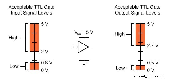
Voltage Tolerance of TTL Gate Inputs
TTL devices run from a nominal 5 V supply (±0.25 V). A perfect TTL “high” would be exactly 5.00 V and a perfect “low” 0.00 V, but actual thresholds are more forgiving:
- Low‑input tolerance: 0 V to 0.8 V
- High‑input tolerance: 2 V to 5 V
Correspondingly, the output guarantees are:
- Low‑output range: 0 V to 0.5 V
- High‑output range: 2.7 V to 5 V
Voltages between 0.8 V and 2 V fall in the "uncertain" zone—TTL manufacturers do not promise how a gate will react to such inputs.
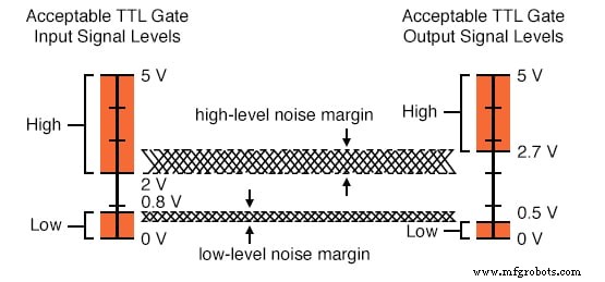
TTL Noise Margin
The noise margin is the buffer between the guaranteed output swing and the acceptable input window. For TTL:
- Low‑level margin: 0.8 V – 0.5 V = 0.3 V
- High‑level margin: 2.7 V – 2 V = 0.7 V
These margins protect a receiving gate from misinterpreting a weak output when cascaded.
Voltage Tolerance of CMOS Gate Inputs
CMOS devices, also typically powered from 5 V, have sharper thresholds but wider margins:
- Low‑input tolerance: 0 V to 1.5 V
- High‑input tolerance: 3.5 V to 5 V
Output guarantees are even tighter:
- Low‑output range: 0 V to 0.05 V
- High‑output range: 4.95 V to 5 V
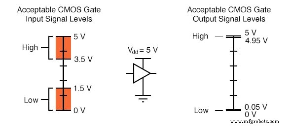
CMOS Noise Margin
CMOS gates boast noise margins of 1.45 V for both low and high levels—more than twice the TTL maximum of 0.7 V—making them resilient to spurious voltage spikes.
Noise Margins at Higher Operating Voltages
Unlike TTL, CMOS can operate from 5 V up to 15 V (some devices even 18 V). Higher supply rails expand the safe input and output windows:
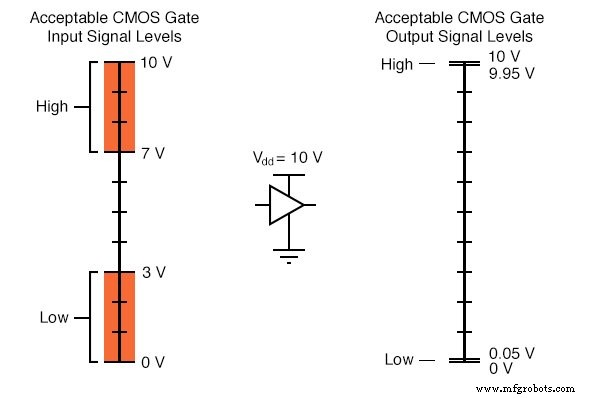
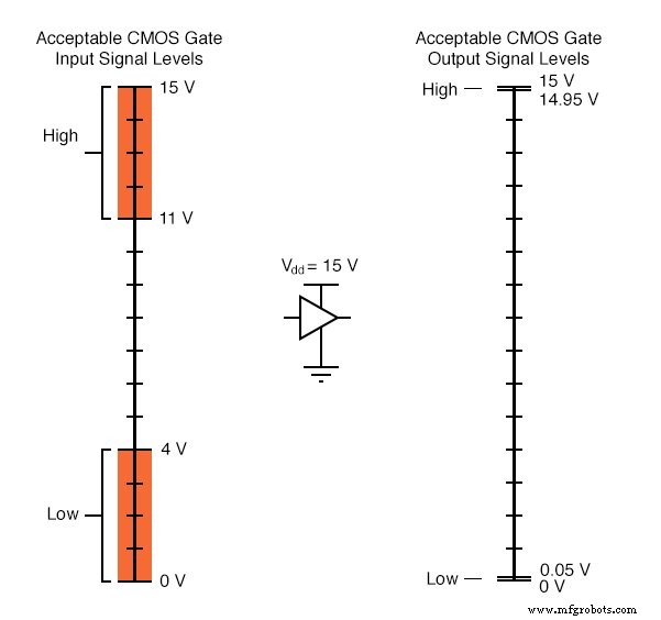
These figures represent worst‑case manufacturer specifications; in practice many CMOS gates tolerate higher “high” signals and lower “low” signals than listed.
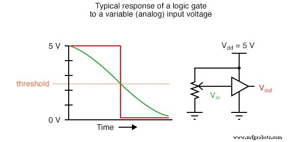
Voltage Thresholds
Within the uncertain input band lies a precise threshold voltage that determines whether a gate interprets the signal as a 0 or a 1. For most devices this threshold is a single point between the highest guaranteed low input and the lowest guaranteed high input.
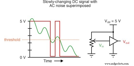
Inputs with AC Noise
When AC noise overlays a DC logic level, the gate can flip back and forth around that single threshold, producing erratic outputs—an issue also seen in analog comparator op‑amps.
Schmitt Trigger
The solution is positive feedback, creating two distinct thresholds: a rising‑edge (VT+) and a falling‑edge (VT–). This hysteresis ensures a stable output even when the input jitters near the decision point.
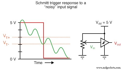
Hysteresis in Schmitt Trigger Gates
Schmitt trigger gates are marked by a small hysteresis symbol in schematics. The built‑in positive feedback boosts noise immunity, making them ideal for noisy environments.
Using TTL and CMOS Technologies in the Same System
While both families can share a 5 V supply, TTL outputs often fall short of CMOS input thresholds when operating at higher voltages, and vice‑versa. Mismatches can cause logic errors.
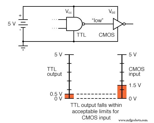
Sample TTL and CMOS Combination Circuit
Consider a TTL NAND gate feeding a CMOS inverter, both powered from 5 V:
• TTL low output (0 V–0.5 V) is comfortably within the CMOS low‑input range (0 V–1.5 V).
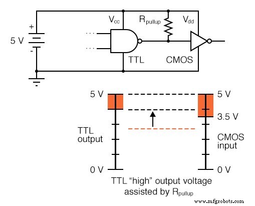
• TTL high output (2.7 V–5 V) may sit in the uncertain zone for CMOS, risking misinterpretation as a low.
Adding a pull‑up resistor on the TTL output can raise the high level to the supply rail, ensuring a solid CMOS high.
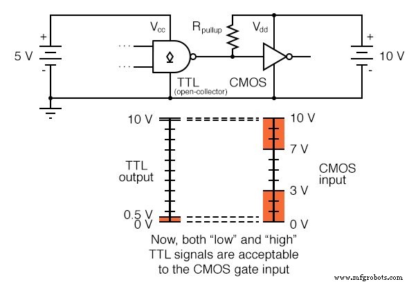
Using an Open‑Collector TTL Gate with a CMOS Gate
Open‑collector TTL outputs can be driven by a pull‑up to any voltage, including 10 V. The resulting high level equals the pull‑up supply, aligning perfectly with a CMOS input operating at that voltage.
Problems of Using CMOS Output to a TTL Input
CMOS outputs are typically safe to feed into TTL inputs when both use the same 5 V supply, because the CMOS high voltage is within the TTL high input window. However, if the CMOS device runs above 5 V, its high output will exceed the TTL high input limit, potentially damaging the TTL gate.
Using Open‑Collector Inverter Circuit
A discrete NPN transistor can emulate an open‑collector inverter, allowing a CMOS high (above 5 V) to be safely translated to a TTL low, and a CMOS low to a TTL high. The logic is inverted, so the system design must account for this.
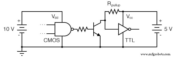
The optional pull‑up resistor lets the TTL input float high when the transistor is off, matching TTL’s default high state.
RELATED WORKSHEET:
- Digital Logic Signals Worksheet
Industrial Technology
- Exploring Voltage Addition with Series Battery Connections
- Voltage Divider Lab: Design, Measurement, and Kirchhoff’s Voltage Law Verification
- Thermoelectricity: Understanding Thermocouples and the Seebeck Effect
- Potentiometric Voltmeter: Precise Voltage Measurement with Minimal Loading
- Build a Potato Battery: A Step‑by‑Step Guide to DIY Electrochemical Power
- Signal Coupling: Understanding AC Noise in Telephone Cables
- Voltage‑to‑Current Signal Conversion: A Practical Transconductance Amplifier Design
- Voltage Signal Systems: Accurate Measurement of Water Tank Levels
- Tachogenerators: Precision Speed Measurement for Industrial Motors and Equipment
- Understanding AC Waveforms: Sine Waves, Frequency, and Oscilloscope Basics