


Special-Purpose Diodes: Schottky, Tunnel, LED, Laser, Photodiode, and Solar Cell Innovations
Schottky Diodes
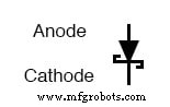
Schottky diodes are metal‑to‑N junction devices, also known as hot‑carrier diodes. They offer exceptionally fast switching, a low reverse‑recovery time, a forward voltage drop of 0.25–0.4 V for a metal‑silicon junction, and minimal junction capacitance. The schematic symbol is shown below.
Advantages & Limitations
- Lower forward drop and reverse‑recovery time than standard rectifiers → ideal for high‑frequency circuits.
- Higher reverse‑breakdown voltage and current ratings are required for power applications; they are best suited for low‑power switching regulators.
Applications
- High‑speed computer logic and signal processing.
- Switching regulators operating at 100 kHz+ where silicon diodes’ 0.7 V drop would waste power.
- Low‑voltage supplies (e.g., 1 V) where a 0.7 V drop is unacceptable.
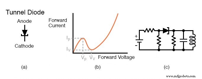
Tunnel (Esaki) Diodes
Tunnel diodes exploit resonant tunneling, producing a negative‑resistance region in their forward‑bias characteristic. When a small forward voltage is applied, current rises to a peak (IP), then falls to a valley (IV), and rises again. The forward voltages at the peak and valley are VP and VV, respectively.
Key Characteristics
- Extremely heavy doping (~1000× higher than rectifiers) → thin depletion region, low breakdown voltage, high capacitance.
- Negative‑resistance region is temperature‑stable, enabling fast switching beyond Schottky diodes.
- Small junction area is required to limit capacitance.
Typical Use Cases
- High‑frequency oscillators (up to 5 GHz) where the diode’s negative resistance drives an LC tank.
- Special microwave circuits and early satellite transmitters (1960s–70s).
Light‑Emitting Diodes (LEDs)
Principle of Emission
LEDs generate photons when electrons recombine with holes in a PN junction. The emitted wavelength is set by the semiconductor bandgap; common combinations include GaAsP (red), GaN (blue), and phosphor‑converted blue (white).
Electroluminescence & Forward Voltage
- Forward drop ranges from 1.6 V (infrared) to >3 V (violet/UV).
- Typical operating current: ~20 mA for standard LEDs; larger devices may use higher currents.
- Series resistors are required when driving from a supply higher than the LED’s Vf to limit current.
Example: With a 6 V supply and a 1.6 V LED, a 220 Ω resistor drops 4.4 V at 20 mA, dissipating 88 mW.
Multiple LEDs
- Parallel strings require individual current‑limiting resistors.
- Series strings share a single resistor but the supply must support the summed Vf.
- Series‑parallel configurations balance efficiency and brightness.
Reverse‑Bias Protection
LEDs have low reverse‑breakdown voltage (~5 V). When powered by AC, an anti‑parallel diode or LED protects the device. The AC half‑cycles then light two LEDs in opposite directions.
Specifications Table
| LED | λ (nm) | Vf (from) | Vf (to) |
|---|---|---|---|
| Infrared | 940 | 1.2 | 1.7 |
| Red | 660 | 1.5 | 2.4 |
| Orange | 602–620 | 2.1 | 2.2 |
| Yellow, Green | 560–595 | 1.7 | 2.8 |
| White, Blue, Violet | - | 3 | 4 |
| Ultraviolet | 370 | 4.2 | 4.8 |
LED vs. Incandescent
- LEDs deliver >3× the lumen/watt of incandescent lamps.
- Longer service life (100,000 h vs. 1,000 h).
- Fast switching enables optical data transmission.
- Monochromatic output can be blended into white LEDs via phosphor or RGB combinations.
Efficiency & Lifespan Comparison
| Lamp type | Lumen/Watt | Life (h) | Notes |
|---|---|---|---|
| White LED | 35 | 100,000 | Costly |
| White LED, future | 100 | 100,000 | R&D target |
| Incandescent | 12 | 1,000 | Inexpensive |
| Halogen | 15–17 | 2,000 | High‑quality light |
| Compact fluorescent | 50–100 | 10,000 | Cost‑effective |
| Sodium vapor, low pressure | 70–200 | 20,000 | Outdoor |
| Mercury vapor | 13–48 | 18,000 | Outdoor |
Laser Diodes
A laser diode builds on LED technology by incorporating an optical cavity, producing coherent, monochromatic light. The laser light remains highly focused over long distances because all emitted photons share the same frequency and phase.
Laser diodes are used in:
- Surveying and rangefinding (straight, non‑diffusing beam).
- Optical storage (CD/DVD/Blu‑ray).
- Fiber‑optic communication.
Operating modes:
- Continuous‑wave: requires a current‑regulating circuit within a narrow current window.
- Pulsed: high‑power short bursts, often for high‑output devices.
Photodiodes
Photodiodes are optimized to generate a current in response to incident light. Silicon is the most common material, though germanium and GaAs are also used. A shallow P‑layer allows most photons to reach the depletion region where electron‑hole pairs are created.
Key operating modes:
- Photovoltaic (PV) mode: small output, low noise below 100 kHz.
- Photocurrent (PC) mode: reverse bias or zero bias; current is linearly proportional to light intensity, ideal for high‑speed applications.
PIN Photodiodes
With an intrinsic layer between P and N regions, PIN diodes reduce capacitance, increase speed (up to tens of GHz), and enlarge the photosensitive volume.
Avalanche Photodiodes (APDs)
APDs apply high reverse bias (10–2,000 V) to amplify the photocurrent via impact ionization. They offer high gain but also higher noise and cost, making them suitable for niche high‑speed, low‑light applications such as single‑photon counting.
Solar Cells
Solar cells convert sunlight into electrical power, operating in photovoltaic mode. They come in several forms, each with trade‑offs in efficiency, cost, and application.
Monocrystalline Silicon Cells
Manufactured by pulling a single‑crystal boule from molten silicon, then slicing into wafers. The N‑type diffusion layer is formed on the wafer surface, and a textured front surface traps light. Back‑contact designs (e.g., SunPower’s 21.5 % cells) increase active area and efficiency.
Multi‑crystalline Silicon Cells
Molten silicon is cast into a block, solidifying into several large crystals. Grain boundaries reduce efficiency, but anti‑reflective coatings mitigate losses. Suitable for most terrestrial installations.
Triple‑Layer (Multi‑junction) Cells
Stacked or monolithic layers with bandgaps tuned to UV (GaInP, 1.8 eV), near‑IR (GaAs, 1.4 eV), and far‑IR (Ge, 0.7 eV) absorb light sequentially. Current‑matching yields voltages summing to ~2.7 V. Commercial space cells reach 32 % efficiency; terrestrial versions target 40.7 % with concentrators.
Process example: Metal‑organic CVD deposits GaInP, GaAs, and Ge layers onto a Ge substrate, each absorbing its designated spectral range.
Thin‑Film Alternatives
- Amorphous silicon: ~13 % max efficiency, 5–7 % after aging, better in low light, used in calculators.
- Cadmium telluride (CdTe): ~16 % efficiency, low‑cost substrates (glass or metal).
- Copper indium gallium selenide (CIGS): ~18 % efficiency, flexible polymer roll‑to‑roll fabrication.
- Organic polymer cells: ~4.5 % efficiency, research stage.
Performance Summary
| Cell type | Max eff. | Practical eff. | Notes |
|---|---|---|---|
| Silicon single crystal (commercial) | 24 % | 14–17 % | $5–$10/peak W |
| Silicon single crystal (space) | 25 % | — | High cost |
| Triple‑junction (space) | 32 % | — | Preferred for space |
| Triple‑junction (terrestrial) | — | 40.7 % | Concentrator‑based |
| CdTe (polycrystalline) | 16 % | — | Glass or metal |
| CIGS (polycrystalline) | 18 % | 10 % | Flexible polymer |
| Amorphous Si | 13 % | 5–7 % | Degrades in sunlight |
Key Takeaways
- Schottky diodes excel in high‑frequency, low‑power switching.
- Tunnel diodes provide ultra‑fast negative resistance for microwave oscillators.
- LEDs and laser diodes offer efficient, controllable light for illumination and communication.
- Photodiodes, especially PIN and APD types, enable sensitive light detection in optical links.
- Solar cell technologies span monocrystalline, multicrystalline, multi‑junction, and thin‑film, each balancing efficiency, cost, and application niche.
Further Reading
- Design Project: Telegraph System Worksheet
- Optoelectronic Worksheet
- Sources of Electricity Worksheet
- Special Diodes Worksheet
Industrial Technology
- Exploring Voltage Addition with Series Battery Connections
- Voltage Divider Lab: Design, Measurement, and Kirchhoff’s Voltage Law Verification
- Thermoelectricity: Understanding Thermocouples and the Seebeck Effect
- Potentiometric Voltmeter: Precise Voltage Measurement with Minimal Loading
- Build a Potato Battery: A Step‑by‑Step Guide to DIY Electrochemical Power
- Low‑Voltage AC Power Supply: Phase‑Shift Circuit Components & Best Practices
- Voltage Regulator Experiment with a 12‑Volt Zener Diode
- Zener Diodes Explained: Voltage Regulation, Design Principles, and Practical Applications
- Tachogenerators: Precision Speed Measurement for Industrial Motors and Equipment
- Understanding AC Waveforms: Sine Waves, Frequency, and Oscilloscope Basics