Industrial manufacturing
Nanomaterials

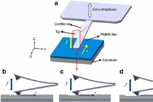
Abstract We demonstrate that dynamic plowing lithography (DPL) performed with an atomic force microscope (AFM) tip can generate dense arrays of nanoscale pits on a poly(methyl methacrylate) (PMMA) thin film at unprecedented speeds. By scratching the surface at high lateral velocities in tapping mode
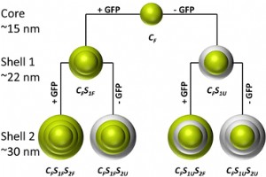
AbstractWe report a streamlined, one‑pot synthesis that yields monodisperse green fluorescent protein (GFP)‑doped silica nanoparticles with diameters ranging from 15 to 35 nm. The method employs L‑arginine‑catalysed sol‑gel chemistry in a biphasic cyclohexane/water system, allowing GFP to be selecti
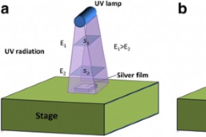
AbstractInkjet‑printed silver gate electrodes were fabricated using a UV‑curing method that delivers an exceptional electrical resistivity of 6.69 × 10⁻⁸ Ω·m. By systematically varying the UV curing time and the distance (D) between the sample and the UV lamp, we identified optimal conditions that m
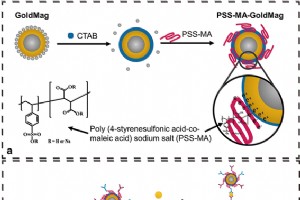
AbstractGold magnetic nanoparticles (GoldMag) have attracted great attention due to their unique physical and chemical performances combining those of individual Fe3O4 and Au nanoparticles. Coating GoldMag with polymers not only increases the stability of the composite particles suspended in buffer
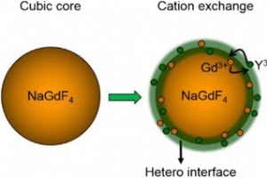
AbstractHexagonal NaREF₄ (RE = Y, Gd, Lu) fluorides are the benchmark hosts for lanthanide‑doped upconversion (UC) nanomaterials, offering crystal lattices that promote intense, photostable emission. Yet, the cubic (α) phase normally dominates at low temperatures, hindering the production of small,
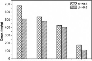
Abstract We report a cost‑effective, scalable synthesis of silica aerogel–supported hydrozincite and Zn/Al carbonate‑hydrotalcite, which exhibit ultra‑thin layers (<5 nm), high surface areas (≈260 m² g⁻¹), and weak crystallinity. Batch adsorption tests against Pb(II) reveal maximum capacities of 684
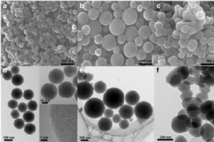
AbstractCarbon nanospheres with distinct microstructures were synthesized by carbonizing F108/resorcinol‑formaldehyde composites followed by KOH activation. The amount of triblock copolymer Pluronic F108 determines the resulting morphology: polydisperse carbon nanospheres (PCNS) with a microporous n
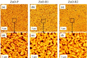
AbstractWurtzite ZnO films were grown on MgO(111) substrates by plasma-assisted molecular beam epitaxy (MBE). Different initial growth conditions were designed to monitor the film quality. All the grown ZnO films show highly (0001)-oriented textures without in-plane rotation, as illustrated by in si
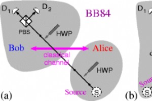
AbstractWe consider attacks on two-way quantum key distribution protocols in which an undetectable eavesdropper copies all messages in the message mode. We show that under the attacks, there is no disturbance in the message mode and that the mutual information between the sender and the receiver is
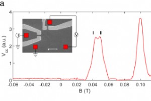
Abstract We report on transverse electron‑focusing (TEF) experiments carried out in an n‑type GaAs two‑dimensional electron gas (2DEG). In a modest transverse magnetic field (B⊥), electrons are steered from a quantum‑wire injector to a detector, producing a series of periodic focusing peaks in B⊥. R
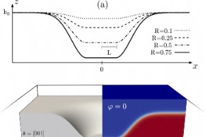
AbstractLateral ordering of heteroepitaxial islands is routinely achieved by pit‑patterning of the substrate prior to deposition. Controlling the shape, orientation and depth of these pits is non‑trivial because the metastable geometries evolve during annealing or subsequent growth. In this work we
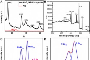
AbstractNovel MoS2/acetylene black (AB) composite was developed using a single-step hydrothermal method. A systematic characterization revealed a few-layered, ultrathin MoS2 grown on the surface of AB. The inclusion of AB was found to increase the capacity of the composite and achieve discharging ca
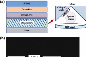
AbstractWe investigated how the sputtering angle and time of indium tin oxide (ITO) influence the morphology and performance of methylammonium lead triiodide (MAPbI3) perovskite films. Increasing the oblique sputtering angle from 0° to 80° enlarged perovskite grain size, a consequence of altered su
Abstract\nThis study investigates the biocompatibility of self‑organized TaOx nanotube arrays produced by electrochemical anodization, with diameters ranging from 20 to 90 nm. All as‑anodized samples were confirmed to be amorphous. Surface wettability varied with nanotube diameter, following Wenzel’
AbstractWe have fabricated high‑quality, atomically thin WS₂ films with single‑domain sizes exceeding 400 µm on Si/SiO₂ substrates using a single‑step atmospheric‑pressure chemical vapor deposition (AP‑CVD) process. By systematically optimizing precursor selection, chamber pressure, growth temperatu
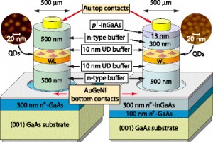
AbstractThe study investigates how the GaAs substrate and its adjacent layers influence the photovoltage (PV) of vertical metamorphic InAs/InGaAs quantum dot (QD) structures, compared with conventional pseudomorphic InAs/GaAs QDs. Structures were grown by molecular beam epitaxy (MBE) with bottom con

AbstractWhile TiO₂ has long been a staple in photocatalysis, its wide band gap (3.2 eV) limits absorption to ultraviolet light, which constitutes only about 4% of solar energy. Recent advances focus on tailoring TiO₂’s optical properties, often by coupling it with a secondary metal‑oxide semiconduct
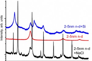
AbstractIn the 2–5 nm size range, nanodiamond exhibits three distinct Raman bands at 1325, 1600, and 1500 cm−1 when excited with a 458‑nm laser. Switching to a 257‑nm laser shifts the 1500‑cm−1 band to 1630 cm−1. Unlike sp2-bonded carbon, the relative intensities of these bands are invariant across
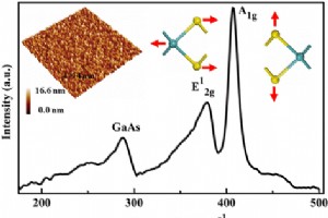
AbstractWe report a record lateral photovoltaic effect (LPE) in molybdenum disulfide (MoS₂) thin films deposited on n‑type GaAs via DC magnetron sputtering. The MoS₂/n‑GaAs heterojunctions display a linear photovoltage that rises to 208.2 mV when the laser spot is near the electrodes, corresponding
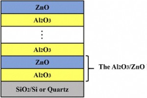
Abstract This study investigates how varying bilayer thickness in Al₂O₃/ZnO nanolaminates influences morphology, optical transparency, and electrical conductivity. Using atomic‑layer deposition (ALD), we fabricated five nanolaminate series (25/25 nm, 10/10 nm, 5/5 nm, 2/2 nm, 1/1 nm) and analyzed th
Nanomaterials