Industrial manufacturing
Nanomaterials

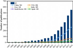
AbstractOver the past two decades, nanomaterials and nanotechnologies (NNs) have profoundly reshaped wastewater treatment. Bibliometric methods offer an objective lens through which the evolving scientific landscape can be charted. In this study, we applied rigorous bibliometric techniques to 2,604
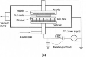
AbstractHydrogenated nanocrystalline silicon (nc‑Si:H) is a leading candidate for high‑performance flat‑panel displays, photodetectors, and solar cells. Its multiphase nature, however, introduces voids and dangling bonds that limit device efficiency. We present a straightforward, high‑pressure PECVD
Abstract 92 % of its initial fluorescence after 2 weeks of storage. Real‑water samples (well, lake, tap) were quantified with recoveries between 95.4 % and 101.6 % and relative standard deviations below 2 %. This FRET platform offers a robust, reusable, and environmentally friendly solution for moni
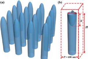
AbstractWe report a new class of semiconductor nanowire (NW) arrays featuring hemiellipsoid and inverted hemiellipsoid caps on gallium arsenide (GaAs) nanowires. The cap geometry simultaneously enhances antireflection and scatters incident light, resulting in exceptional light confinement even with
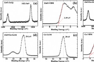
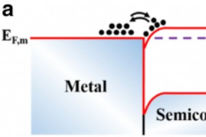
AbstractWe present a systematic study of metal–insulator–semiconductor (MIS) contacts on n‑Ge that incorporates a thin ZnO interfacial layer (IL) to suppress Fermi‑level pinning (FLP) at the metal/Ge interface. A modest conduction band offset of 0.22 eV between ZnO and n‑Ge is observed, which, toget
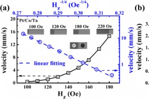
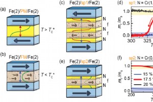
AbstractWe investigate how the insertion of a carbon interlayer affects the Dzyaloshinskii–Moriya interaction (DMI), current‑induced domain wall (DW) velocity, and tilting in Pt/Co/Ta racetracks. Magneto‑optical Kerr microscopy reveals that the DMI strength is dominated by the Pt/Co interface, remai
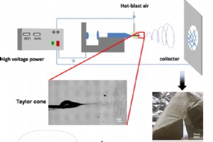
AbstractElectrospinning provides an effective method for generating nanofibers from solution of carboxymethyl chitosan/polyoxyethylene oxide (CMCS/PEO). The goal of this work is to explore the potential application of electrospun CMCS/PEO nanofiber membrane in fruit fresh-keeping. The microstructure
AbstractUnmethylated cytosine‑phosphate‑guanine (CpG) oligodeoxynucleotides are potent toll‑like receptor 9 (TLR9) agonists that stimulate a Th1‑biased immune response, offering promise as cancer therapeutics or vaccine adjuvants. Unfortunately, CpG is rapidly degraded by nucleases and shows limited
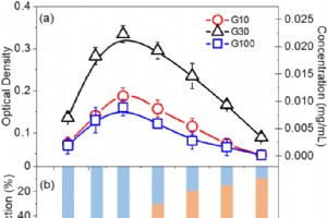
AbstractGraphene nanoplatelets (GNPs) can be efficiently produced by exfoliating graphite in liquid media using high‑power tip sonication. In this work, three commercially available flaked graphite grades were sonicated at 60, 100, 200, or 300 W for 10, 30, 60, 90, 120, or 180 min. The resulting GNP
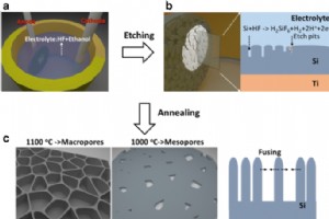
AbstractWe report a high‑performance electrochemical double‑layer supercapacitor (EDLC) electrode comprising few‑layer graphene‑passivated porous silicon (PSi). The PSi matrix was fabricated by electrochemical etching of a p‑type silicon wafer, followed by Ni‑assisted chemical vapor deposition (CVD)
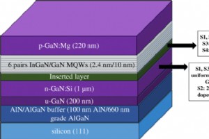
Abstract This study investigates the photoluminescence performance of InGaN/GaN multiple‑quantum‑well (MQW) LEDs grown on silicon substrates. The devices incorporate distinct tensile‑stress‑controlling architectures—periodic silicon δ‑doping in the n‑type GaN layer or insertion of InGaN/AlGaN spacer
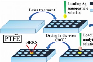
AbstractSurface‑enhanced Raman scattering (SERS) delivers single‑molecule sensitivity, making it an attractive optical sensor for diverse fields. Yet, high‑cost fabrication and complex processing hinder its industrial uptake. Here we report a simple, inexpensive approach that uses CO2 laser ablation
AbstractMechanisms of the recently demonstrated ex-situ thermal control of the indirect exchange coupling in magnetic multilayer are discussed for different designs of the spacer layer. Temperature-induced changes in the hysteresis of magnetization are shown to be associated with different types of
AbstractUltra-wide bandgap beta-gallium oxide (β-Ga2O3) has been attracting considerable attention as a promising semiconductor material for next-generation power electronics. It possesses excellent material properties such as a wide bandgap of 4.6–4.9 eV, a high breakdown electric field of 8 MV/cm,
Abstract Hybrid organic–inorganic and all‑inorganic lead halide perovskites have emerged as leading candidates for next‑generation optoelectronics. Two‑dimensional (2D) Ruddlesden–Popper (RP) variants are particularly attractive because their band gaps can be tuned by layer thickness, enabling preci
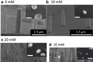
Abstract We investigate the role of ammonium hydroxide (NH4OH) as a growth additive in the hydrothermal synthesis of ZnO nanowires (NWs) on seed‑free Au substrates. By systematically varying NH4OH concentrations (0–50 mM), we achieve more than a two‑order‑of‑magnitude change in NW density. Photolumi
AbstractUsing a straightforward hydrothermal route, we engineered hierarchical SnO₂ nanoflowers whose morphology is tuned by surfactants. When polyvinyl‑pyrrolidone (PVP) is introduced, the resulting flower‑like architecture is highly porous and exhibits outstanding sensing toward ethanol and H₂S.
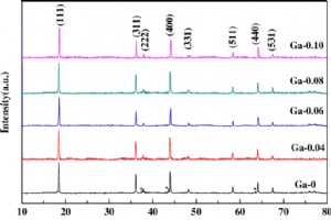
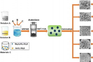
AbstractUsing a sol‑gel route, LiNi0.5−xGaxMn1.5O4 (x = 0, 0.04, 0.06, 0.08, 0.10) cathodes were synthesized and systematically studied. X‑ray diffraction confirms a disordered Fd3m spinel phase; gallium doping suppresses the LixNi1−xO secondary phase and increases cation disorder, which improves el
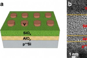
AbstractThis study demonstrates that a single V/SiOx/AlOy/p++Si resistive memory cell can operate as either a selector or a memory element simply by tuning the compliance current limit (CCL). When a low CCL of 1 µA is applied during a positive forming step, the device exhibits unidirectional thresho
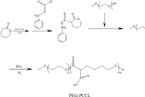
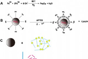
AbstractConventional chemotherapy often fails to achieve therapeutic concentrations at tumor sites because of physiological barriers, leading to suboptimal efficacy and systemic toxicity. Nanocarriers that encapsulate hydrophobic drugs can overcome these hurdles by improving drug solubility, prolong
Nanomaterials