

Industrial manufacturing
Industrial Technology

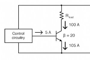
Insulated‑gate field‑effect transistors (IGFETs) achieve virtually infinite current gain because their gate is isolated from the channel. No continuous gate current is drawn; only a brief transient is needed to charge the gate‑channel capacitance and shift the depletion region as the device switches

What is a MESFET?A metal‑semiconductor field‑effect transistor (MESFET) is a high‑frequency transistor that uses a gallium arsenide (GaAs) or indium phosphide (InP) channel to achieve lower noise, higher speed, and higher power density than silicon devices.Key BenefitsExceptional transconductance an
Insulated‑Gate Field‑Effect Transistors (IGFETs), the backbone of modern CMOS and analog circuits, can exhibit subtle but critical quirks that affect performance, reliability, and yield. Below are the most frequent issues, their underlying physics, and proven strategies to keep your designs running
Choosing the Right Transistor Ratings and Packages for IGFETs Integrated Gate Field‑Effect Transistors (IGFETs), commonly known as MOSFETs, are the backbone of modern power electronics. To guarantee performance, safety, and longevity, engineers must carefully match a device’s electrical ratings and
Introduction Ion‑Gate Field‑Effect Transistors (IGFETs) form the backbone of modern analog and digital circuits. Proper biasing is essential to ensure linearity, maximize gain, and minimize power consumption. Drawing on 15+ years of semiconductor design experience, this guide distills proven biasing
Common‑Gate IGFET Amplifier The common‑gate (CG) configuration is a fundamental building block in high‑frequency analog design. With the source terminal tied to the input signal and the gate held at a fixed bias, the device delivers a near‑unity voltage gain and exceptionally low input impedance—id
What Is a Common‑Drain IGFET? A common‑drain amplifier, also known as a source‑follower, is a simple but powerful configuration used in MOSFET and IGFET circuits. It offers a voltage‑unity gain, very high input impedance, and low output impedance, making it ideal for buffering and impedance matching
Common‑Source Amplifier (IGFET) The common‑source (CS) stage is the workhorse of MOSFET (IGFET) amplifier design. It delivers the highest voltage gain among the three basic MOSFET topologies, making it ideal for audio, RF, and mixed‑signal applications. Key Characteristics Voltage Gain (Av) ≈ –gm·
Indium Gallium Arsenide Field‑Effect Transistors (IGFETs) are the backbone of high‑speed RF and mixed‑signal ICs. When operated in the active mode, an IGFET behaves as a voltage‑controlled resistor, providing high transconductance, low on‑resistance, and excellent linearity. Key Principles of Active
Enhancement‑Mode IGFETs Enhancement‑mode insulated‑gate field‑effect transistors (IGFETs) are the backbone of contemporary CMOS logic, RF amplifiers, and power electronics. Unlike depletion‑mode devices, they remain non‑conductive until a positive gate bias turns them on, offering superior control o
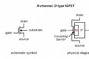
Insulated gate field‑effect transistors (IGFETs) are unipolar devices, much like JFETs: the controlled current flows entirely within a single type of semiconductor, so no PN junction is crossed by the current. Inside the device, a PN junction exists solely to form the non‑conducting depletion region
In the previous chapter we examined several field‑effect transistor architectures. The junction field‑effect transistor (JFET) modulates channel conductivity by varying the depletion width of a reverse‑biased PN junction with applied voltage. The insulated‑gate field‑effect transistor (IGFET) operat
Decoding JFET Quirks: Common Pitfalls & How to Master Them Field‑effect transistors (FETs) are ubiquitous in analog design, yet the junction‑gate FET (JFET) often surprises even seasoned engineers with subtle quirks. This guide distills the most frequent pitfalls, explains why they happen, and shows
JFET Transistor Ratings & Package OverviewJump‑gate field‑effect transistors (JFETs) are cornerstone components in low‑noise, high‑impedance analog circuits. This guide reviews the most critical electrical ratings, thermal limits, and package styles you’ll encounter, helping you match a device to yo
Understanding JFET BiasingJunction Field‑Effect Transistors (JFETs) are prized for their high input impedance and low noise. However, achieving optimal performance requires careful biasing to set the correct gate‑to‑source voltage (VGS) and drain‑to‑source current (ID). This guide outlines the most
RELATED WORKSHEETS: JFET Amplifiers Worksheet What Is a Common‑Gate JFET Amplifier? The common‑gate (CG) configuration is one of the three classic JFET topologies (common‑source, common‑drain, common‑gate). In the CG stage the gate is the common terminal, the source is the input, and the drain is
What is a Common‑Drain JFET Amplifier? The common‑drain configuration, also called a source follower, is a widely used JFET topology that delivers high input impedance, low output impedance, and near‑unity voltage gain. This makes it ideal for buffering, level shifting, and impedance matching in ana
Common‑Source JFET Amplifier Overview The common‑source configuration is the workhorse of JFET amplifier design. By biasing the gate at a negative voltage relative to the source, the device operates in the saturation region, providing high voltage gain while maintaining a high input impedance. Key E
Junction‑field‑effect transistors (JFETs) behave much like bipolar junction transistors (BJTs) in that they can operate in an active regime—between cutoff and saturation—where they regulate current. To illustrate this behavior, we’ll run a SPICE simulation that mirrors the one used to study basic BJ
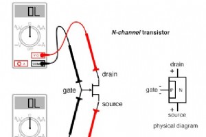
Testing a JFET with a multimeter can seem simple at first glance, because the device contains only one PN junction—between gate and channel. However, measuring the drain‑to‑source path is a bit more involved, especially when the transistor’s internal capacitance can hold a residual charge that keep
Industrial Technology

The Fabrication Industry Explained: Processes, Materials, and Impact
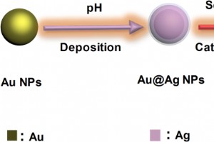
Efficient Charge Transfer in Au/CdSe Janus Nanoparticles Boosts Photocatalytic Hydrogen Production

12 Proven Practices for a Successful CMMS Implementation
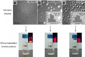
Optimizing Emulsion Droplet Size and PVA Surfactant to Enhance Stability of Quantum‑Dot Micellar Nanocrystals
