

Industrial manufacturing
Industrial Technology

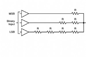
The R/2R ladder DAC is a popular alternative to the traditional binary‑weighted (R/2ⁿR) converter, offering a simpler resistor set‑up without sacrificing performance. R/2R vs. R/2ⁿR DAC Traditional binary‑weighted designs require a unique resistor value for each bit—often eight different resistors f
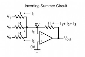
What Is a R/2nR DAC Circuit? The R/2nR DAC—often called a binary‑weighted input DAC—is a specialized form of the inverting summing amplifier. It converts a set of binary input voltages into a single analog voltage whose magnitude is proportional to the binary number represented. In a standard invert
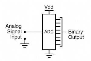
Integrating digital circuitry with sensor devices is straightforward when the sensors themselves are digital—switches, relays, and encoders naturally interface with gate logic because their signals are binary on/off. When analog devices enter the picture, the interface becomes considerably more invo
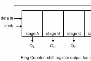
A ring counter is a special type of shift register where the output of the last stage is fed back into the first. When clock pulses are applied, the data pattern circulates indefinitely. For instance, in a four‑stage ring counter the pattern repeats every four clock pulses, but the register must fir
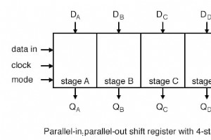
A parallel‑in/parallel‑out shift register accepts data in parallel, shifts it, and presents the shifted result, as illustrated below. A universal shift register expands this capability by supporting parallel loading, serial shifting, and additional control options such as direction and hold modes. &
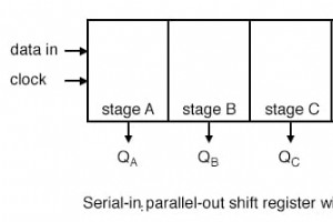
A serial‑in, parallel‑out (SIPO) shift register shares the data‑shifting core of its serial‑in, serial‑out counterpart, but it exposes every internal stage as a separate output pin. This makes it an ideal solution for converting a single serial data line into multiple parallel outputs. How It Works
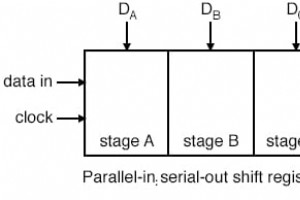
Parallel‑to‑Serial (PISO) shift registers expand the functionality of serial‑in/serial‑out (SISO) devices by allowing all stages to load data simultaneously. This capability is essential for converting parallel data—each bit on its own wire—into a serial stream for efficient communication. A PISO re
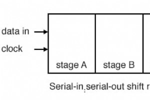
Shift registers that receive data serially and output it serially are a cornerstone of digital logic design. They delay each bit by one clock period per stage, enabling precise data buffering, serial communication, and clock‑domain crossing. Each stage stores a single bit, so a single‑stage register
Shift registers are a cornerstone of sequential logic circuits, functioning similarly to counters but with a focus on data flow rather than counting. Unlike combinational logic, which reacts solely to present inputs, sequential logic retains a memory of past events. This memory capability allows shi
Until now we have focused on combinational logic, where outputs depend solely on current inputs. In many real‑world applications, circuits must retain a memory of past inputs and adjust their outputs accordingly. Such circuits are known as sequential circuits. This article walks through the end‑to‑e

Incomplete
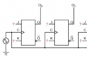
What Is a Synchronous Counter? A synchronous counter differs from an asynchronous (ripple) counter in that all output bits change state simultaneously. By tying every flip‑flop’s clock input to the same clock pulse, we avoid the ripple delay that characterizes ripple counters. When using J‑K flip‑fl
Previously we examined a single J‑K flip‑flop configured to count backwards in a two‑bit binary sequence (11 → 10 → 01 → 00). To build a counter that increments forward, we must analyze the forward count pattern and determine how to interconnect multiple flip‑flops. Binary counters rely on a factor
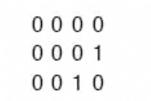
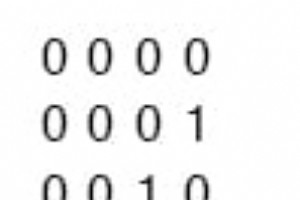
When examining a four‑bit binary count sequence—from 0000 to 1111—a clear pattern emerges in the way each bit oscillates between 0 and 1. The least significant bit (LSB) toggles every count step, while each higher‑order bit flips at half the frequency of its predecessor. Consequently, the most sign
We’ve already encountered a monostable multivibrator in practice: the pulse detector inside a flip‑flop that momentarily powers the latch during a clock edge. A pulse detector is classified as a monostable multivibrator because it has only one stable output state. In this state the device holds its
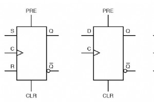
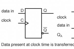
In digital design, the primary data inputs of a flip‑flop—whether D, SR, or JK—are termed synchronous because their influence on the outputs (Q and ΔQ) manifests only on a clock edge. In contrast, the additional inputs we call asynchronous—preset (PRE) and clear (CLR)—can force the flip‑flop
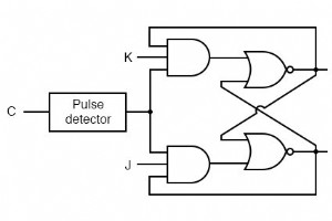
The J‑K flip‑flop is a refined bistable multivibrator that resolves the classic S‑R latch’s invalid state. By integrating feedback into the set (S) and reset (R) inputs, it guarantees a valid output for every input combination. In the diagram below, notice how the traditional 2‑input AND gates have
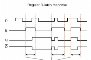
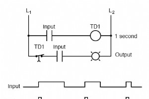
In earlier sections we examined S‑R and D latches that respond to data inputs only when an enable (E) signal is active. For many digital designs, it is advantageous to confine the latch’s responsiveness to a very brief interval rather than to the entire duration that the enable line remains high. Ed
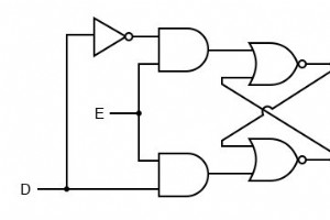
In a gated S‑R latch, the enable pin allows the Q and Q̅ outputs to remain latched regardless of the S or R signals. By removing one of those inputs, we obtain a multivibrator latch that eliminates any illegal state. Such a circuit is called a D latch, and its internal logic looks like this:
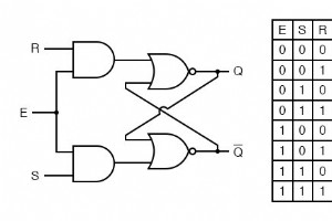
In digital logic design, a gated SR latch is a versatile memory element that updates its state only when a dedicated enable input allows it. This feature is invaluable for preventing unintended state changes and adding an extra layer of control in complex circuits. The enable pin, often labeled E or
Industrial Technology
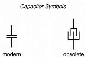
Electric Fields and Capacitors: Fundamentals, Functionality, and Design

Breaking Down Lithium Battery Costs: Why They’re More Expensive Than You Think
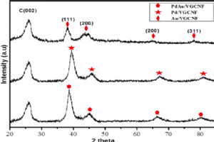
PdAu Nanoparticle Catalysts on Vapor‑Grown Carbon Nanofibers: Performance in Passive Direct Glycerol Fuel Cells

How 3D Printing Enhances Traditional Manufacturing: Five Proven Applications
