Industrial manufacturing
Industrial Technology


Read‑only memory (ROM) shares many design principles with RAM, but its latching mechanism is engineered for a single, irreversible write cycle. The most basic ROM uses tiny fuses that can be selectively blown to encode binary information; once a fuse is ruptured, the data cannot be altered, making t
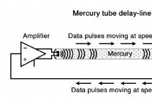
In the formative years of computing, designers pushed beyond mechanical relays and vacuum tubes, pioneering nonmechanical storage solutions that would shape modern memory architecture. One of the most inventive concepts was the delay line. A delay line delays the propagation of a pulse or wave—much
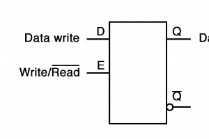
Digital storage has evolved beyond mechanical solutions. Today’s primary memory types—static RAM (SRAM), dynamic RAM (DRAM), and flash—rely on solid‑state circuitry, offering high speed, reliability, and zero moving parts. SRAM: Bistable Multivibrators in a Compact Array At the core of SRAM lies the
When we store information in a circuit or device, we need a reliable way to store, retrieve, and precisely locate where that data resides. Most memory devices can be visualized as a series of mailboxes, file‑cabinet folders, or any metaphor that illustrates how information can be found in multiple p
While many textbooks cover digital memory fundamentals, this chapter offers a distinctive exploration of both legacy and contemporary technologies in depth. Digital memory’s core purpose is to store and retrieve binary data—sequences of 1s and 0s—providing benefits analogous to digital over analog c
Industrial control systems demand rapid, predictable data delivery. When a nuclear reactor’s coolant valve is governed by a digital network, every command must arrive within a strict time window – a failure to do so can lead to catastrophic outcomes. Determinism: The Guarantee of Timing In networki
Beyond the physical attributes of a network—signal types, voltage levels, connector pinouts, cabling, and topology—there must be a clear, standardized method for managing communication among multiple nodes, even in a simple two‑node point‑to‑point link. When a node transmits, it imposes a signal on
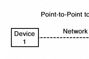
Point‑to‑Point Connecting two digital devices directly creates a dedicated link known as a point‑to‑point topology. The wiring is represented as a single line between the two endpoints, but the underlying media can be twisted‑pair copper, coaxial cable, optical fiber, or even a seven‑conductor Bogus
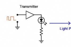
Introduction Modern networks increasingly rely on light to carry digital data. Instead of converting binary signals into electrical voltage swings, optical transmitters (LEDs or solid‑state lasers) generate pulses of light that can be received by photodiodes or phototransistors, enabling a seamless
In the BogusBus system, each of the five signal wires carried a single binary bit: 0 V denoted “off” and 24 V DC represented “on.” Because all bits arrived simultaneously, BogusBus is classified as a parallel network. Adding binary encoding at the transmitter and decoding at the receiver—so that mor
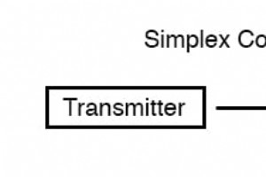
Buses and networks are engineered to enable seamless communication between interconnected devices. The movement of information—known as data flow—can manifest in various patterns. In simplex communication, data travels only one way—from a designated transmitter to a designated receiver. The BogusBu
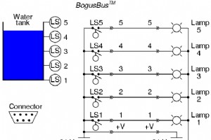
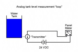
The wires between the tank and the monitoring location is called a bus or a network. The distinction between these two terms is more semantic than technical, and the two may be used interchangeably for all practical purposes. In my experience, the term “bus” is usually used i
When engineering large and complex digital systems, reliable data exchange between devices is essential. Digital signals inherently resist transmission errors far better than their analog counterparts, ensuring greater integrity and clarity. These benefits manifest in the crystal‑clear quality of di
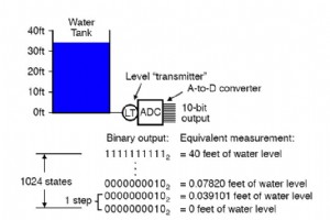
In any data‑acquisition system, the most critical ADC parameter is its resolution—the number of binary states it can produce. Because an ADC converts a continuously varying analog input into a finite set of digital codes, knowing how many distinct levels exist is essential. For example, a 10‑bit ADC
Delta‑sigma (ΔΣ) analog‑to‑digital converters (ADCs) represent a sophisticated family of devices that transform continuous voltage signals into high‑resolution digital data. In mathematics and physics, the Greek capital letter Δ stands for difference or change, while Σ denotes summation. The ΔΣ arch
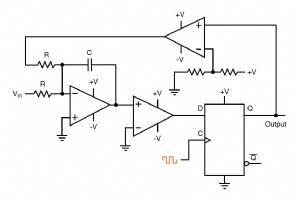
While flash ADCs excel in speed, their large component count can be prohibitive for many designs. A common strategy to reduce complexity is to replace the DAC‑based ramp of a flash ADC with an analog integrator and a precise digital counter, yielding what is known as a single‑slope or integrating AD
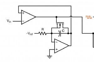
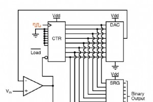
A third variation on the counter‑DAC based converter theme is, in my view, the most elegant. Instead of a conventional “up” counter driving the DAC, this design uses an up/down counter. The counter runs continuously, and the up/down control line is driven by the comparator’s output. When the analog
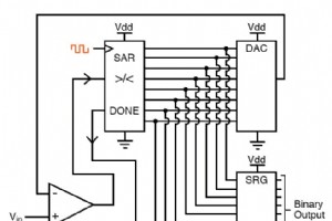
One effective solution to the limitations of a digital ramp ADC is the successive‑approximation ADC. The core innovation lies in a specialized counter called the successive‑approximation register (SAR). Rather than incrementing through a binary sequence from zero to full scale, the SAR sets each bit
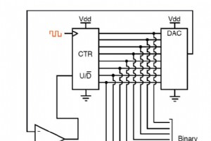
Often called a stairstep‑ramp or simply a counter ADC, the digital ramp converter is conceptually straightforward but has inherent performance constraints. The core idea is to feed a free‑running binary counter into a digital‑to‑analog converter (DAC), then compare the DAC’s analog output with the s
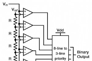
Also known as a parallel A/D converter, the flash ADC is the most straightforward ADC architecture. It consists of a series of comparators, each comparing the analog input to a distinct reference voltage. The comparator outputs feed a priority encoder that generates a binary output. The diagram belo
Industrial Technology